Особенности разгона современных процессоров Intel для LGA1150
Возможность разгона процессоров уже многие годы является их неотъемлемой частью. Конечно, с ростом производительности эта процедура стала менее востребованной, но своей актуальности все же не утратила. Центральный процессор до сих пор остается основным компонентом ПК, в связи с чем остальные комплектующие в системе очень сильно зависят от его быстродействия. Причем, чем выше уровень конфигурации, тем сильнее сказывается эта зависимость. Вторая причина, заставляющая пользователей смотреть в сторону разгона процессора, заключается в недостаточной оптимизации программного обеспечения. Так, купив многоядерный процессор, вы еще не гарантируете обеспечение максимальной производительности. Например, в играх не редки случаи, когда модель с меньшим количеством ядер, но большей частотой, показывает лучшие результаты, чем ее более дорогой аналог.

Таким образом, чтобы там не говорили скептики, оверклокинг на сегодняшний день не является просто развлечением, а несет реальную практическую пользу. В этих словах мы уже неоднократно убеждались, тестируя процессоры разной производительности. Однако в рамках обычного обзора трудно рассказать обо всех нюансах, касающихся процесса оптимизации параметров. Поэтому данному вопросу мы решили посвятить отдельный материал, вернее сказать, цикл материалов. Первой его частью станет эта статья, где мы постараемся в полной мере раскрыть особенности разгона современных процессоров компании Intel. Речь пойдет о моделях, основанных на микроархитектуре Intel Haswell: семействах Intel Haswell, Intel Haswell Refresh, Intel Devil’s Canyon и Intel Haswell-E.
Способы разгона
Суть оптимизации параметров процессора в подавляющем большинстве случаев сводится к увеличению его тактовой частоты. В современных решениях от Intel она вычисляется по формуле:
CPU Freq = CPU Ratio × CPU Cores Base Freq
- CPU Freq − частота процессора;
- CPU Ratio − процессорный множитель;
- CPU Cores Base Freq − базовая частота процессорных ядер.
В связи с этим можно выделить три основные способа их разгона:
- путем изменения процессорного множителя;
- путем изменения опорной частоты;
- путем одновременного изменения процессорного множителя и опорной частоты.
Во время оверклокинга также требуется настройка массы дополнительных параметров, затрагивающих работу не только самого процессора, но и других структурных узлов ПК (подсистемы оперативной памяти, чипсета, слотов расширения, интерфейсов). Более того, нужно постоянно отслеживать основные показатели всей конфигурации и на каждом этапе проверять стабильность ее функционирования.
Чтобы избавить пользователя от большинства из этих обязанностей, производители материнских плат предлагают инструменты автоматического разгона процессоров.

Как правило, они реализованы на уровне драйвера.

. или же доступны в виде специального раздела в меню BIOS.

В некоторых случаях для этих целей даже предусмотрена специальная группа кнопок, распаянных непосредственно на текстолите.
Вроде бы, основная цель достигнута − производительность процессора увеличена, и на этом материал можно заканчивать. Но у автоматического способа разгона есть много недостатков, которые выявляются в процессе повседневной эксплуатации. Во-первых, он нередко завышает многие параметры для обеспечения стабильной работы системы, тем самым излишне нагружая другие компоненты ПК. В результате конфигурация потребляет больше энергии, требует лучшего охлаждения и издает дополнительный шум. Во-вторых, материнская плата содержит лишь несколько профилей оверклокинга. Поэтому разогнать процессор до той отметки, которая требуется именно вам, не всегда получится. Придется довольствоваться только значениями, предусмотренными производителем. Более того, в некоторых случаях у системы может попросту не получиться подобрать необходимые параметры (например, при использовании решения с заблокированным множителем) и никакого ощутимого прироста от процедуры оверклокинга вы не получите. В-третьих, использование определенных функций вместе с автоматическим разгоном может быть затруднено. Особенно это касается тонкой настройки режимов энергосбережения. В-четвертых, в автоматическом режиме вы никогда не сможете достичь тех показателей и результатов, которые будут продемонстрированы при ручной оптимизации параметров.
Исходя из этого, мы рекомендуем отказаться от автоматического способа оверклокинга в пользу ручного. Однако для начала потребуются определенные знания о принципе работы процессора и подконтрольных ему узлов, а также способы его взаимодействия с другими комплектующими. Об этом мы поговорим в следующем разделе.
Особенности функционирования современных процессоров Intel. Анализ работы структурных элементов, задействованных во время процедуры разгона
Более детально об особенностях микроархитектуры Intel Haswell и Intel Haswell-E можно узнать, перейдя по соответствующим ссылкам. Здесь же внимание будет акцентировано на структурных элементах, касающихся разгона.

Самым главным из них является базовая (или опорная) частота тактового генератора (BCLK), которая по умолчанию равна 100 МГц. Как видно из схемы, все узлы процессора (процессорные ядра, кэш-память последнего уровня, встроенное графическое ядро, кольцевая шина, контроллеры памяти, шин PCI Express и DMI) так или иначе с ней связаны. Поэтому любое изменение опорной частоты неминуемо отразится на их работе. Причем, если процессорные ядра без проблем переносят такую процедуру, то другие узлы процессора и компоненты ПК могут терять стабильность своего функционирования при значении базовой частоты, которое всего лишь на несколько мегагерц превышает отметку в 100 МГц. Иными словами, разгон процессора по базовой частоте, по сути, просто лимитируется остальными узлами системы.
Чтобы решить сложившуюся проблему, в микроархитектуру Intel Haswell было внедрено понятие CPU Strap − множитель опорной частоты процессорных ядер. Таким образом, имеем следующее:
CPU Cores Base Freq = CPU Strap × BCLK Freq
- CPU Cores Base Freq − базовая частота процессорных ядер;
- CPU Strap − множитель опорной частоты процессорных ядер;
- BCLK Freq − опорная частота BCLK.

Как правило, для параметра CPU Strap доступны четыре значения: 1,00; 1,25; 1,66 и 2,5. Но и их хватит с головой для максимального разгона процессора по опорной частоте. Поскольку при стандартном значении BCLK (100 МГц) базовая частота процессорных ядер может достигать 250 МГц при использовании максимального множителя CPU Strap. То есть теоретически скорость процессора можно увеличить в 2,5 раза, не меняя его множителя. Владельцы решений из серий Intel Sandy Bridge / Ivy Bridge о таком могли только мечтать.
Правда, потенциальным покупателям современных моделей на основе микроархитектуры Intel Haswell тоже не стоит сильно обольщаться. Параметр CPU Strap доступен только для процессоров с разблокированным множителем (с индексом «K» в конце названия). Иными словами, обычные решения в данном случае тоже не смогут похвастать большим оверклокерским потенциалом − максимум +5. +10 МГц к опорной частоте BCLK без потери стабильности работы всей системы, что даст прибавку в скорости в виде дополнительных 150 − 400 МГц в зависимости от процессорного множителя.

Отметим, что параметр CPU Strap можно использовать двумя способами. В первом случае его значение фиксируется вручную, а во втором − подбирается автоматически материнской платой на основе желаемой базовой частоты опорных ядер процессора. Допустим, мы хотим, чтобы наша частота CPU Cores Base Freq была равна 150 МГц. На основе этого значения материнская плата сама определит, что параметр CPU Strap нужно зафиксировать на уровне 1,66, что даст нам скорость BCLK (BCLK Freq) на уровне 90,3 МГц (150 МГц / 1,66 = 90,3 МГц). Правда, стоит понимать, что стабильная работа системы при этом тоже не гарантируется. Зато так проще производить оптимизацию, поскольку фактически мы меняем только один параметр (скорость работы процессорных ядер). Тогда как в ручном режиме придется производить манипуляцию уже с двумя настройками (CPU Strap и базовая частота BCLK).
Теперь давайте вкратце пройдемся по узлам процессора и комплектующим ПК, скорость работы которых тактируется базовой частотой BCLK. Самыми чувствительными к изменению этого значения являются встроенные в процессор контроллеры памяти, линий PCI Express и шины DMI, служащие для «общения» с внешними компонентами системы (оперативной памятью, картами расширения и чипсетом соответственно). Поэтому очень важно позаботиться об их стабильной работе. Достигается это с помощью увеличения напряжения питания на конкретных узлах, а также путем отключения энергосберегающих технологий (более детально об этом читайте в следующих разделах).

В современных процессорах часто на кристалле распаивается графическое ядро. Скорость его работы рассчитывается по формуле:
iGPU Freq = iGPU Ratio × BCLK Freq / 2
- iGPU Freq − частота встроенного графического ядра;
- iGPU Ratio − множитель встроенного графического ядра;
- BCLK Freq − опорная частота BCLK.
Из-за архитектурных особенностей, встроенное графическое ядро чуть лучше «переваривает» повышенные значения базовой частоты BCLK, особенно при увеличении напряжения на нем. Однако в большинстве случаев в составе современных ПК используется дискретная видеокарта, в связи с чем встроенная графика автоматически деактивируется. Тем самым убирается один из компонентов, который может лимитировать разгон процессора. Еще одной положительной стороной отказа от использования iGPU является снижение нагрева процессора. К примеру, разгон встроенного графического ядра Intel HD Graphics 4600 с номинальных 1250 МГц до 1700 МГц приводит к росту энергопотребления модели Intel Core i7-4770K в среднем на 40 Вт.

Для расчета скорости оперативной памяти используется следующая формула:
Memory Freq = Memory Ratio × BCLK Freq × Memory Strap
- Memory Freq − частота оперативной памяти;
- Memory Ratio − множитель оперативной памяти;
- BCLK Freq − опорная частота BCLK;
- Memory Strap − делитель между опорной частотой и скоростью работы оперативной памяти.
Как видим, в данном случае мы также имеем два множителя (или делителя, смотря относительно каких величин анализировать). Первый (Memory Ratio) задает непосредственно коэффициент умножения для скорости подсистемы оперативной памяти. Второй же (Memory Strap) указывает на соотношение опорной частоты BCLK к базовой частоте модулей оперативной памяти. По сути, этот параметр является аналогом CPU Strap, только для оперативной памяти. Правда, в данном случае доступно уже меньше значений (в основном только 1,00 и 1,33). Использование значения 1,33 позволяет устанавливать более низкий множитель (Memory Ratio) и запускать память с меньшими таймингами. Таким способом можно улучшить показатели при прохождении определенных синтетических тестов, критических к задержкам модулей. Но с другой стороны, от этого страдает стабильность работы всего ПК. Поэтому при разгоне процессора оптимальное соотношение опорной частоты BCLK к базовой скорости планок оперативной памяти все же будет 1,00.

Последним важным структурным компонентом, напрямую зависящим от опорной частоты BCLK, является блок Uncore, объединяющий в себе кольцевую шину и кэш-память последнего уровня процессора. В микроархитектуре Intel Haswell их пропускная способность существенно увеличена (примерно в 2 раза), поэтому нет больше необходимости использовать модуль Uncore на высоких частотах. Кроме того, разработчики добавили возможность управлять его работой независимо от процессорных ядер. То есть эти два структурных блока (стек физических ядер и кэш-память) могут функционировать на разных частотах. Большинство оверклокеров сходятся во мнении, что при сильном разгоне процессора, скорость Uncore лучше устанавливать примерно на 300 − 500 МГц меньше частоты самого процессора. Хотя в некоторых синтетических бенчмарках синхронизация этих показателей, наоборот, позволяет добиться более высоких результатов. Как бы там ни было, нужно помнить, что оптимизация на уровне скорости блока Uncore осуществляется не для достижения стабильности работы системы после разгона процессора, а для увеличения показателей производительности.
Расчет частоты кольцевой шины и скорости кэш-памяти осуществляется по следующей формуле:
Uncore Freq = Uncore Ratio × BCLK Freq
- Uncore Freq − скорость работы модуля Uncore;
- Uncore Ratio − множитель частоты работы модуля Uncore;
- BCLK Freq − опорная частота BCLK.
Особенности регулятора питания современных процессоров Intel. Анализ напряжений, которые используются во время процедуры разгона
Изменение схемы работы структурных узлов процессора, как правило, требует корректировки их рабочих напряжений. То же самое касается остальных комплектующих, находящихся в тесной связи с процессором (оперативная память и чипсет). Можно, конечно, положиться на материнскую плату и предоставить ей возможность в автоматическом режиме подобрать необходимые значения. Но, опять же, такая оптимизация будет далека от оптимальной и не позволит добиться максимальных результатов разгона.
Поэтому рекомендуем запастись терпением и разобраться в электротехнической части процессоров, основанных на микроархитектуре Intel Haswell.

Как видно из представленной выше схемы, их ключевой особенностью является отказ от полностью внешнего регулятора питания, ведь часть его перекочевала внутрь процессора (iVR). Теперь на входе процессора модуль VRM (расположен на материнской плате) формирует одно напряжение Vccin, которое в дальнейшем превращается в номиналы, необходимые для питания конкретных узлов. Такое техническое решение позволило увеличить качество выходных напряжений (в частности, уменьшить пульсации) и повысить эффективность самого преобразователя. С другой стороны, iVR занимает часть полезного пространства на кристалле и продуцирует дополнительное тепло. Но это уже особенности микроархитектуры Intel Haswell, которые не имеют прямого отношения к процедуре разгона процессора.
Итак, какие же нам напряжения пригодятся во время оптимизации параметров современных решений от Intel? Для лучшей наглядности приведем их в виде списка:
- Vccin (VRIN) − входное напряжение питания процессора;
- Vcore − напряжение питания на ядрах процессора;
- Vring (Vuncore, Vcache) − напряжение питания на модуле Uncore (кольцевой шине и кэш-памяти последнего уровня);
- Vigpu (Vgfx) − напряжение питания на встроенном в процессор графическом ядре;
- Vsa (VCCSA) − напряжение питания на системном агенте, которое, по сути, является напряжением питания на контроллере памяти (используется при увеличении скорости работы подсистемы оперативной памяти);
- Vioa / Viod − напряжения питания на узлах, связанных с работой встроенного контроллера памяти (используются при увеличении скорости работы подсистемы оперативной памяти);
- Vddq (Vdram) − напряжение питания на модулях оперативной памяти.
Разбираемся с настройками меню BIOS
На наш взгляд, наиболее удобным и универсальным инструментом для разгона процессора является меню BIOS, поскольку программное обеспечение, работающее в среде операционной системы, имеет сравнительно ограниченный функционал.
В данном разделе мы постараемся по максимуму осветить настройки BIOS, которые могут пригодиться во время оверклокинга, а также дать конкретные рекомендации по выбору значений для тех или иных параметров. Хотим обратить ваше внимание, что основной акцент сделан на разгоне процессора, а процедуре оптимизации параметров той же самой подсистемы оперативной памяти будет посвящена отдельная статья. Ну и напоследок хочется сказать, что приведенные ниже рекомендации в основном касаются неэкстремального оверклокинга с применением традиционных систем охлаждения (воздушный кулер, СВО).
Настройки, касающиеся частоты работы структурных узлов процессора и сопутствующих комплектующих
Если после входа в BIOS загрузилось упрощенное меню, советуем сразу же переключиться в расширенный режим. Это сделает доступными все настройки, касающиеся разгона комплектующих и мониторинга основных показателей состояния системы. Как правило, интересующие нас опции группируются на отдельных вкладках, носящих характерные названия: «OC Tweaker» (ASRock), «Extreme Tweaker» (ASUS), «M.I.T.» (GIGABYTE), «OC» (MSI).

Здесь и далее в таблице приводятся названия настроек, которые наиболее часто встречаются в меню BIOS материнских плат. Для более детального ознакомления с возможностями каждой опции предлагаем посетить наш справочник по настройкам BIOS.
Рекомендации по использованию
BCLK Frequency (ASUS), BCLK/PCIE Frequency (ASRock), Host/PCIe Clock Frequency (GIGABYTE), CPU Base Clock (MSI)
Задает базовую (опорную) частоту BCLK
Подобрать такое значение, при котором система сохраняет стабильность своей работы и показывает максимальную производительность.
CPU Core Ratio (ASUS / GIGABYTE), CPU Ratio (ASRock), Adjust CPU Ratio (MSI)
Задает процессорный множитель
Подобрать такое значение, при котором система сохраняет стабильность своей работы и показывает максимальную производительность.
Если материнская плата позволяет задать максимальный множитель для каждого ядра отдельно, рекомендуем во всех случаях устанавливать одинаковые значения (синхронизировать скорость всех ядер).
CPU Strap (ASUS), Processor Base Clock / Gear Ratio (GIGABYTE), Adjust CPU Base Clock Strap
Задает делитель между опорной частотой BCLK и базовой частотой процессорных ядер
Для неэкстремального разгона, как правило, можно ограничиться значениями [1,00] и [1,25]. Поскольку, чем больше значение базовой частоты процессорных ядер, тем меньший процессорный множитель удастся выставить до появления проблем со стабильностью работы системы.
CPU Base Clock (GIGABYTE)
Изменяет опорную частоту процессорных ядер
Данная настройка доступна не на всех платах. Суть ее заключается в том, что вы изначально меняете только опорную частоту процессорных ядер, а такие параметры как скорость BCLK и делитель CPU Strap подбираются автоматически. Такой способ является более удобным и простым, поэтому если в меню BIOS присутствует соответствующая опция, рекомендуем ею воспользоваться.
Max. CPU Cache Ratio (ASUS), CPU Cache Ratio (ASRock), Uncore Ratio (GIGABYTE), Adjust Ring Ratio (MSI)
Устанавливает множитель частоты модуля Uncore (кольцевой шины и кэш-памяти последнего уровня)
Значение стоит подбирать так, чтобы в случае незначительного разгона процессора частота работы модуля Uncore была примерно на 0 − 300 МГц меньше скорости процессорных ядер, а при сильном разгоне − меньше на 300 − 500 МГц.
DRAM Frequency (ASRock / ASUS, MSI)
Задает скорость работы оперативной памяти
Подобрать такое значение, при котором система сохраняет стабильность своей работы и показывает максимальную производительность. Обращаем ваше внимание, что список значений формируется автоматически на основе множителей, которые используются при расчете скорости оперативной памяти. Причем последние не всегда доступны для регулировки.
System Memory Multiplier (GIGABYTE)
Задает множитель базовой частоты оперативной памяти
По сути, то же самое, что и настройка DRAM Frequency, только в этом случае скорость оперативной памяти задается не простым выбором частоты, а путем установки необходимого множителя. При этом материнская плата сразу же показывает расчетную скорость модулей.
BCLK Frequency: DRAM Frequency Ratio (ASUS), DRAM Reference Clock (MSI)
Задает делитель между опорной частотой BCLK и базовой частотой оперативной памяти
Используется для точной настройки частоты оперативной памяти во время разгона. Также может пригодиться для достижения рекордных результатов в специфических синтетических тестах.
В обычной же ситуации рекомендуем использовать значение
Max. CPU Graphics Ratio (ASUS), Adjust GT Ratio (MSI)
Задает множитель базовой частоты встроенного графического ядра
Подобрать такое значение, при котором система сохраняет стабильность своей работы и показывает максимальную производительность. Если использование встроенной графики не планируется, лучше оставить значение
GT Frequency (ASRock), Processor Graphics Clock (GIGABYTE)
Задает частоту встроенного графического ядра
Используется для тех же целей, что и опции Max. CPU Graphics Ratio (ASUS), Adjust GT Ratio (MSI). Разница кроется лишь в том, что здесь частота задается не через множитель, а явно.
Если использование встроенной графики не планируется, лучше оставить значение
Настройки, касающиеся напряжений, которые используются для корректной работы структурных узлов процессора и сопутствующих комплектующих
Перед тем, как перейти к непосредственному анализу настроек, стоит отметить, что напряжения питания на большинстве материнских плат могут задаваться несколькими способами:
- В автоматическом режиме, когда значения устанавливаются по умолчанию.
- В ручном режиме, когда точное значение напряжения питания вводится вручную.
- В offset-режиме, когда точное значение напряжения питания задается вручную с помощью offset-параметра (величина, на которую будет увеличено/уменьшено номинальное напряжение питания).
- В адаптивном режиме, когда напряжение питания задается вручную с помощью offset-параметра и/или специально отведенной для этих целей опции. При этом оно может динамически меняться в зависимости от частоты работы узла и характера текущей нагрузки на него для улучшения стабильности работы системы или уменьшения энергопотребления. Данный способ рекомендуем использовать для постоянной работы с разогнанным процессором, после того как в ручном режиме уже были подобраны оптимальные настройки.

Для некоторых напряжений питания доступен только один способ их регулировки, для других − сразу все четыре. Какой из них использовать, зависит только от ваших личных предпочтений и возможностей материнской платы. Мы же для упрощения в таблице укажем названия лишь для ручного способа (исключением являются те опции, для которых предусмотрен только offset-режим) установки значений напряжения питания.
Рекомендации по использованию
CPU Input Voltage (ASRock / ASUS), CPU VRIN External Override (GIGABYTE), VCCIN Voltage (MSI)
Задает входное напряжение питание процессора (Vccin / VRIN)
Данное значение всегда должно быть выше остальных напряжений питания, использующихся узлами процессора. В большинстве случаев для неэкстремального оверклокинга достаточно значения, лежащего в пределах 1,7 − 2,0 В. Для использования разогнанного процессора на постоянной основе рекомендуем не превышать отметки 2,2 В.
CPU Core Voltage Override (ASUS), Vcore Override Voltage (ASRock), CPU Vcore Voltage (GIGABYTE), CPU Core Voltage (MSI)
Задает напряжение питания на процессорных ядрах (Vcore)
В большинстве случаев для неэкстремального оверклокинга достаточно значения, лежащего в пределах 1,10 − 1,35 В. Для использования разогнанного процессора на постоянной основе рекомендуем не превышать отметки 1,38 В.
CPU Cache Voltage Override (ASUS), CPU Cache Override Voltage (ASRock), CPU RING Voltage (GIGABYTE, MSI)
Задает напряжение питания на модуле Uncore: кольцевой шине и кэш-памяти последнего уровня (Vring / Vuncore / Vcache)
Поднятие этого напряжения питания даже без увеличения частоты Uncore часто помогает достигнуть стабильной работы процессора при разгоне. В большинстве случаев для неэкстремального оверклокинга достаточно значения, лежащего в пределах 1,10 − 1,25 В. Для использования разогнанного процессора на постоянной основе рекомендуем не превышать отметки 1,30 В.
CPU Graphics Voltage Override (ASUS), GT Voltage Offset (ASRock), CPU Graphics Voltage (GIGABYTE), CPU GT Voltage (MSI)
Задает напряжение питания на встроенном в процессор графическом ядре (Vigpu / Vgfx)
Следует изменять только в случае разгона встроенного в процессор графического ядра. Как правило, достаточно значения, лежащего в пределах 0,90 − 1,35 В. Дальнейшее увеличение напряжения не оправдано, поскольку практически не влияет на стабильность работы iGPU на высоких частотах.
CPU System Agent Voltage Offset (ASUS / GIGABYTE), System Agent Voltage Offset (ASRock), CPU SA Voltage Offset (MSI)
Задает напряжение питания на системном агенте, которое, по сути, является напряжением питания на контроллере памяти (Vsa / VCCSA)
Используется при увеличении скорости работы подсистемы оперативной памяти. Если акцент делается на разгоне процессора, то рекомендуем устанавливать значение
CPU Analog I/O Voltage Offset (ASRock / ASUS / GIGABYTE / MSI)
Задает напряжения питания на узлах, связанных с работой встроенного контроллера памяти (Vioa / Viod)
Используется при увеличении скорости работы подсистемы оперативной памяти. Как показывает практика, в обоих случаях лучше оставлять значение
CPU Digital I/O Voltage Offset (ASRock / ASUS / GIGABYTE / MSI)
DRAM Voltage (ASRock / ASUS / GIGABYTE / MSI)
Задает напряжение питания на модулях оперативной памяти
Используется при увеличении скорости работы подсистемы оперативной памяти. Если акцент делается на разгоне процессора, то рекомендуем выбирать параметр
PCH Core Voltage (ASUS), PCH 1.05V Voltage (ASRock / MSI), PCH Core (GIGABYTE)
Задает напряжение питания на чипсете
Изменение этого напряжения питания позволяет улучшить стабильность работы системы при увеличении опорной частоты BCLK. Как правило, достаточно выставить значение в пределах 1,05 − 1,15 В.
PCH VLX Voltage (ASUS), PCH 1.5V Voltage (ASRock / MSI), PCH IO (GIGABYTE)
Задает напряжение питания на модуле в чипсете, отвечающего за обмен данными между процессором и чипсетом посредством шины DMI
С помощью данного параметра можно улучшить стабильность работы системы при изменении частоты шины DMI (а иногда и опорной частоты BCLK). Экспериментальным путем установлено, что чем выше ее скорость, тем ниже должно быть значение этого напряжения и наоборот. К примеру, для частоты DMI свыше 120 МГц нужно выставлять значение близкое к 1,05 В, а для частоты меньше 90 МГц − около 1,70 В.
В оверклокерских материнских платах можно обнаружить массу дополнительных напряжений, которые имеет смысл изменять только при экстремальном разгоне. В повседневных же ситуациях эти опции окажутся маловостребованными. Если же вас все-таки заинтересует их предназначение, опять же, рекомендуем обратиться к нашему справочнику по настройкам BIOS.
Дополнительные настройки, позволяющие добиться стабильности работы процессора после его разгона

В современных материнских платах реализовано довольно много технологий, которые так или иначе влияют на работу системы, в том числе и процессора. Пока все компоненты ПК функционируют в «стоковых» режимах, это незаметно. Но вот в процессе оверклокинга их влияние становится более заметным, поэтому иногда оптимизацию полезно проводить и на этом уровне.
Рекомендации по использованию
Load Line Calibration (ASUS), CPU Load Line Calibration (ASRock), CPU VRIN Loadline Calibration (GIGABYTE), CPU Vdroop Offset Control (MSI)
Позволяет скомпенсировать просадки напряжения питания на компонентах процессора, возникающие при увеличении нагрузки на него
При стандартных параметрах или при их незначительной оптимизации стоит устанавливать значения [Medium], [Standart] или [High] (если значения в процентах, то [+25%] или [+50%]), а при экстремальном разгоне есть смысл использовать и более агрессивные настройки − [Ultra High] и [Extreme] (если значения в процентах, то [+75%] или [+100%]). Однако стоит учитывать тот факт, что чем выше значение, тем большим будет нагрев силовых элементов модуля VRM и самого процессора. К тому же выбор неправильного параметра может, наоборот, привести к слишком завышенному напряжению на процессоре, что, опять же, негативным образом скажется на его температуре. Корректность и точность работы технологии Load Line Calibration также зависит и от уровня материнской платы.
PLL Selection (ASUS), Filter PLL Frequency (ASRock), CPU PLL Selection (GIGABYTE), CPU PCIE PLL (MSI)
Отвечает за выбор метода фильтрации сигнала тактового генератора опорной частоты BCLK
При поднятии опорной частоты BCLK рекомендуется выбирать метод [SB PLL]
Filter PLL (ASUS / MSI), Filter PLL Level (GIGABYTE)
Позволяет активировать дополнительные методы фильтрации сигнала тактового генератора опорной частоты BCLK
При сильном поднятии опорной частоты BCLK (свыше 170 МГц) следует устанавливать параметр [High BCLK], в противном случае − оставлять значение по умолчанию (
BCLK Amplitude (ASUS / MSI)
Позволяет задать амплитуду сигнала тактового генератора опорной частоты BCLK
Увеличение этого значения рекомендуется при сильном поднятии опорной частоты BCLK.
CPU Spread Spectrum (ASUS), Spread Spectrum (ASRock, MSI, GIGABYTE)
Изменяет форму сигнала на системной шине (BCLK), благодаря чему уменьшается уровень электромагнитного излучения и наводок от компонентов системы
При любой, даже незначительной оптимизации параметров системы рекомендуется отключать эту опцию (значение [Disabled]).
EPU Power Saving Mode (ASUS), Power Saving Mode (ASRock), CPU Internal VR Efficiency Management, Intel Turbo Boost Technology, Intel SpeedStep Technology, EIST Technology (ASUS / ASRock / GIGABYTE / MSI) и другие
Отвечают за активацию разнообразных энергосберегающих технологий, как всего процессора, так и его отдельных узлов
Для достижения максимальных результатов во время разгона комплектующих рекомендуется выключать все эти функции (значение [Disabled]).
CPU Integrated VR Current Limit (ASUS), Primary Plane Current Limit (ASRock), Core Current Limit (GIGABYTE), CPU Current Limit (MSI)
Позволяет установить максимальную силу тока, проходящего через встроенный в процессор регулятор питания
В зависимости от степени разгона, следует устанавливать более высокие значения, что отодвинет порог срабатывания «троттлинга» (пропуск тактов) при достижении максимальной величины тока, проходящего через встроенный регулятор питания.
Long Duration Package Power Limit (ASUS / ASRock / GIGABYTE / MSI)
Задает значение максимальной мощности, потребляемой процессором
В зависимости от степени разгона следует устанавливать более высокие значения, что отодвинет порог срабатывания «троттлинга» (пропуск тактов) при достижении максимальной мощности, потребляемой процессором. По умолчанию этот показатель равен TDP процессора.
Short Duration Package Power Limit (ASUS / ASRock / GIGABYTE / MSI)
Задает значение максимально возможного энергопотребления процессора при очень кратковременных нагрузках (не более 10 мс)
Следует устанавливать такое значение, которое не превышает показатель Long Duration Package Power Limit больше, чем на 25%.
CPU Current Capability (ASUS), Thermal Feedback (ASUS), CPU Integrated VR Fault Management (ASUS), CPU Over Voltage Protection (MSI), CPU Over Current Protection (MSI), CPU VRM Over Temperature Protection (MSI), CPU VRIN Current Protection (GIGABYTE), CPU VRIN Thermal Protection (GIGABYTE), CPU VRIN Protection (GIGABYTE) и другие
Расширяет диапазон разнообразных параметров процессора и регуляторов питания (например, силы тока, входного напряжения, допустимых рабочих температур и т.д.)
Данные опции фактически являются защитами от повреждения процессора и других компонентов системы из-за подачи высокого напряжения. Во время оверклокинга допустимые значения стоит увеличивать (либо вовсе отключать некоторые опции), чтобы избежать ситуации, когда материнская плата будет ограничивать возможности разгона.
Intel Adaptive Thermal Monitor (ASUS / ASRock / GIGABYTE / MSI)
Позволяет управлять механизмом защиты процессоров Intel от перегрева
Во время разгона процессора данную опцию лучше отключать (значение [Disabled]), а его нагрев мониторить вручную.
От теории к практике. Разгон процессоров, основанных на микроархитектуре Intel Haswell, на примере модели Intel Core i7-4770K
А теперь пришло время показать, как использовать полученные теоретические знания на практике. Для этого был выбран процессор Intel Core i7-4770K с разблокированным множителем. Остальная конфигурация тестового стенда приведена в таблице:
ASRock Fatal1ty Z97X Killer (версия BIOS 2.00)
Intel Core i7-4770K
SilverStone Heligon SST-HE01 (максимальная скорость вращения вентилятора)
2 x DDR3-2400 TwinMOS TwiSTER 9DHCGN4B-HAWP
AMD Radeon HD 6970
Seagate Barracuda 7200.12 ST3500418AS
Чтобы показать зависимость между параметрами системы во время разгона процессора, были проведены три серии тестов для разных значений опорной частоты процессорных ядер (100, 125 и 166 МГц). В каждом случае мы постепенно увеличивали их множитель и искали минимально возможные показатели напряжения входного питания (VRIN) и напряжения на процессорных ядрах (Vcore), при которых ПК еще сохранял стабильность своей работы (проверка осуществлялась путем прогона стресс-теста). Для комплексного анализа эффективности оптимизации параметров параллельно осуществлялась фиксация нагрева процессора (выбиралась температура самого горячего ядра) и уровень входного энергопотребления (всей конфигурации от розетки). Естественно, все показания снимались под максимальной нагрузкой на CPU.
Опорная частота процессорных ядер − 100 МГц
ASUS MAXIMUS Z690 EXTREME & i9-12900K GUIDE — Load Lines, VF Curves, Adaptive Voltage, By Core & OCTVB
In a world increasingly concerned with natural resources, the watchword is efficiency. So, it's time to look at adaptive voltage and by core with other eyes.
This is not to say that the era of overclocking with "Sync all cores" and "fixed voltage" is over, as it is much easier and faster to do, and brings good results, but it is not "Single Thread" efficient.
It is worth remembering that Intel supplies its processors operating stock in "by core" and "Adaptive Voltage", and now goes beyond, and manufactures its processors with performance cores and efficiency cores.
But anyway, why would I trade the easiest way to overclock it for a more complicated one? The answer is simple, because we like complicated things. Now a day, with the current processing capability, it is not necessary to overclock, and even then we do this complicated thing, just for a few extra frames. So we do it for fun. The overclock itself can be fun like a game. After all, isn't it nice to know that we can go a little over the limit with that hardware we bought?
My thanks to Shamino and Asus for all their support and for inviting me to join the ROG Maximus Z690 platform test team.
My sincere thanks to Falkentyne and Cstkl1 for their help during testing.
Considerations:
The intention of this work is not to provide an overclocking recipe or break records, but to help understand how voltages, frequencies and temperatures work in the octvb configuration.
Asus has great features in its MBs that enable TVB overclocking, but it also provides a unique optimization tool called "AI Overclocking" which works very well.
This guide will cover the basics of Load Lines, By Core Usage, VF Curves, TVB, and OCTVB.
* * * This procedure can be applied to the Z490 / Z590 / Z690 Maximus and Strix MBs with some adjustments. * * *
- My "CPU — Voltage and OCTVB Tool"
- By core
- TVB
- OCTVB
- Adaptive Voltage & VF curve
- Specific Core Adaptive voltage
- Interpolation
- Understanding LLC, AC_LL & DC_LL
- Choosing LLC, AC_LL and DC_LL
- Undestanding the LLC, DC_LL and AC_LL numbers
- The LLC effect
- Setting the Full Load frequency
- Defining Load Lines
- System startup
- Adjusting the minimum voltage to full load P-51x / E-40x
- About E-cores
- Defining the By Core Usage
- System stability test
- ASUS OCTVB
- Understanding Asus OCTVB
- Notes
- Bios Attachments
Here you can download my "CPU — Voltage and OCTVB Tool"
CPU Voltage Tool
CPU Power Specifications:
The "By core" is nothing more than the use of processor cores at different frequencies, depending on the workload.
Below, we find the default frequency settings for some processors:
*Image credits: SkatterBencher
We will use the following nomenclature to refer to the frequencies and numbers of cores:
[frequency] X [number of cores running concurrently] — [frequency] X [number of cores running concurrently] — etc.
Full load means all cores are running at the same time on this frequency:
[Full Load] @ P-[frequency] x / E-[frequency] x
9900K
50×2 – 48×4 – 47×8
Full load @ 47x
10900K
53×2 – 51×4 – 50×6 – 49×10
Full load @ 49x
11900K
53×2 – 52×4 – 51×6 – 49×8
Full load @ 49x
12900K:
P: 52×1 – 51×2 – 50×4 – 49×8
E: 39×4 – 37×8
Full load @ P-49x/E-37x
* Data from an 12900k CPU read by Asus OCTool.
The typical CPU has a standard clock speed and a turbo boost speed. However, CPUs with Thermal Velocity Boost have two additional Boost speeds. Also known as Intel TVB, the feature is available on 10th, 11th, 12th generation desktop chips.
TVB is a technology that takes advantage of the processor's thermal "opportunity" to increase its working frequency.
Thermal Velocity Boost allows these CPUs to achieve even higher boost speeds than their typical turbo boost.
This means that in addition to its standard clock speed and Boost of all cores, an Intel CPU can have four additional speeds.
Turbo Boost 2.0 is a single-core Boost available if the CPU is running to your power, current, and temperature specifications.
The velocity of turbo boost max 3.0 applies to two favorite cores. It is only possible if the CPU is running below its power, current, and temperature specifications.
Thermal Velocity Boost takes the fastest of the two favorite CPU cores at a higher speed than it gets with turbo boost max 3.0.
This is only possible if the CPU is running below 70 degrees Celsius and if the CPU is running below its power, current and temperature specifications.
The thermal speed increase of all cores refers to the reachable speed if all cores are active and the CPU is operating under its respective temperature limit (70 degrees Celsius).
The TVB overclock consists of changing boost patterns to achieve higher frequencies than standard when there is a thermal opportunity.
E.g. You can change the Boost of the 12900k to work this way.
Before +2Boost Profile:
P: 56×2 – 55×3 – 53×5 – 51×8
E: 42×4 – 41×6 – 40×8
Full load @ P-51x/E-40x
After +2Boost Profile:
P: 58×2 – 57×3 – 55×5 – 53×8
E: 42×4 – 41×6 – 40×8
Full load @ P-51x/E-40x
Note:
The Boost Profile will never be applied to the E-Cores.
The Full Load frequency will be the raw "By core" full laod due to temperature.
* Asus OCTool — Intel Monitor
Applying the Boost Profile, several rules are applied to the combination of frequency x cores so that the CPU takes advantage of the low temperature to reach high clocks.
* Asus OCTool -CPU OCTVB
What we simply do is set up a new TVB: if the workload is low, the frequency will be high, and when the workload is high, the frequency will be lower.
Changing TVB, or rather overclocking TVB, we come to Asus OCTVB.
Warning:
For OCTVB to work, you need to enable C-States !
Adaptive Voltage & VF curve:
Unlike the "fixed Voltage", the “Adaptive Voltage" and "VF curve" behaveso as to monitor the frequency.
Higher frequencies require higher voltages, lower frequencies, lower voltages.
Every processor comes standard with an internal VF curve that we can't change.
Asus MBs allow us to add an offset (positive or negative) to these points of the original curve.
So, we can say that Asus allows us to change the “voltage x frequency” CPU curve.
These values can be found in the BIOS on this page:
NOTE:
The default setting for VF #11 is 5300MHz. In the image above, "By core usage" changed this frequency to 55x
And +2Boost Profile changed it again, to 57x.
Asus allows us to change the voltages of all points through the offset and allows us to change the frequency only of the last point through the "By Core usage " setting.
This VF curve shows the voltage that the CPU will use for a specific frequency.
When CPU is running 4800MHz, the VID used will be the VF#6, as well VF#5 is the VID of 4200MHz.
So the CPU is changing the voltage all the time, and these voltages can be modified by some factores like LLC and AC_LL
When we assign a frequency to a number of cores using "By Core Usage", the highest frequency will assume the last point on the VF curve.
Note:
When we apply a Boost, this Boost will be applied to the last point of the VF curve.
Note that the maximum frequency set in "By Core Usage" is 55x.
So why is the last line of the VF curve (VF #11) 57x?
The explanation is easy:
The "Per core usage" is the raw frequency, without any OCTVB boost.
When boost is applied, you will see the higher frequency boosted int the VF curves.
(To see the boosted frequency in the VF curve you need to "save and exit" after selecting the Boost profile and entre BIOS again)
If you want to limit some core frequency, you should limit the raw "By core usage" frequency.
So, in the example below, with +2Boost profile, core 0 and core 1 are limited to 57x (not 55x) and cores 2 and 3 to 56x (not 54x)
If you are using +1Boost profile, core 0 and core 1 will be limited to 56x (not 55x) and cores 2 and 3 to 55x (not 54x)
Therefore, the minimum "By core usage" frequency (51x) will be the full load frequency and the highest will be the highest plus the selected booster.
In this case, the + 2Boost profile was applied.
So, for our TBV overclock, the important points will always be the last two in the VF curve.
The points VF#7 and VF#8 for the 10900K and 11900K and the POINTS VF#7 and VF#11 for the 12900K.
Points VF#8,9 and 10 in the 12900K will not be used and must remain in AUTO.
About ADL VF curve
1-7 are unique points,
11 is OC point (user can change this ratio). This is the only ratio user can change on this curve.
8-10 are copies of 7
7 is the last unique point
The rule appears to be when ratios are the same, point 7 must be >= point 8 otherwise it will MCA
Acode does not like when point 7 voltage offset is less than point 8
If you want to program 7 negative, you must program point 8 negative first
If you want to program point 8 positive, you must program point 7 positive first
If you don't follow this rule then Acode throws MCA
If programming a negative offset to point 7, best way is to start with point 10 and program it negative, then go to 9,8, and 7 programing them all the same negative value
If programming a positive offset to only point 8, best way is to start with 7 and then go to 8,9, and 10 programming them all to the same positive value
Specific Core Adaptive voltage:
The Specific Core Adaptive Voltage is a resource that allows you to set the adaptive voltage individually for each core.
The goal is to set more voltage to the worst cores and less voltage to the best cores.
The Specific Core Adaptive voltage is a step beyond, to be used after you are stable using the global adaptive voltage.
Let’s say we are running the max frequency of 5700MHz and the system is stable with a global adaptive voltage of 1460mv.
So, at this point, we know that 1460mv is enough for the worst cores run 57x.
With this logic, if 1460mv is enough for the worst cores, probably the best cores can run this frequency with less than 1460mv.
But how less? That is what we are going to know.
The first step is to enter BIOS at the IA Optimization page and take note of the P-cores VIDs from Core0 to Core7.
This information will show us the worst core VID. In the example above, core 4.
Now we know this core will need 1460mv to run 57x. All the others cores will be able to run 57x with less voltage.
Now let’s find the voltages we will need to run 57x for the others cores.
The math is simple:
Specific Core Adaptive Voltage = (Global_Adaptive) – [(Worst_Core_VID) – (Core_number_VID + offset_for_this_core)]
So, for the global adaptive of 1460mv (the one that our system is stable) and the specific core VID shown in the bios page above, we will have the following values:
* We will not use any specific core offset now.
Core0 = (1460) – [(1329) — (1299)] = 1430mv
Core1 = (1460) – [(1329) — (1299)] = 1430mv
Core2 = (1460) – [(1329) — (1304)] = 1435mv
Core3 = (1460) – [(1329) — (1304)] = 1435mv
Core4 = (1460) – [(1329) — (1329)] = 1460mv
Core5 = (1460) – [(1329) — (1289)] = 1420mv
Core6 = (1460) – [(1329) — (1319)] = 1450mv
Core7 = (1460) – [(1329) — (1284)] = 1415mv
As you can see at the image below.
So, using these Specific Core Adaptive Voltages you will run as stable as before when you were using the global Adaptive voltage, with the advantage of reducing the Vcore when bad cores are sleeping.
A tip about " Specific Core Adaptive voltage offset".
You can use the Specific Core Adaptive voltage offset to “normalize” the cores voltages as you can see below.
But I don’t think it is the best strategy.
You can download my Excel voltage tool to help you with this math.
CPU Voltage Tool
In mathematics, linear interpolation is a method of curve fitting using linear polynomials to construct new data points within the range of a discrete set of known data points.
We can use interpolation to find a voltage between two VF points, or between the last VF point and the adaptive voltage.
So let take as an example the following VF curve with an OC frequency of 5700MHz:
The 5100MHz VID is in some place between VF#6 (1184) and VF#7 (1299)
To find the estimated 5100MHz VID we will apply the following formula:
5100_VID = (VF#7_VID — VF#6_VID ) / (VF#7_freq — VF#6_freq) * (5100 — VF#6_freq) + VF#6_VID
5100_VID = (1299 — 1184) / (5300 — 4800) * (5100 — 4800) + 1184
5100_VID = (115) / (500) * (300) + 1184
5100_VID = 1253mv
So the estimated VID for 5100MHz will be 1253mv
If you apply a negative offset of 50mv to VF#6 you must use the new VF#6_VID value to find the new 5100_VID
So, in this case, the new 5100_VID is 1245mv.
You can increase or decrease the 5100_VID by changing the VF#6 offset or the VF#7 offset.
Attention here because if you decide to change VF#7 this will have an effect on the interpolation of VF#7 to the adaptive voltage.
The voltage that will be applied at the maximum OC frequency will be the adaptive voltage or VF #11 (whichever is higher).
In this example, the Adaptive is higher than VF#11
Adaptive = 1458
VF#11 + offset = 1445
So now let's find the estimated 5500_VID with a 20mv positive offset applied to VF#7:
VF#7 = 1299
VF#7+offset = 1299+20 = 1319mv
5500_VID = (Adaptive- VF#7_VID+offset) / (OC_Freq — VF#7_freq) * (5500 — VF#7_freq) + VF#7_VID+offset
5500_VID = (1458 — 1319) / (5700 — 5300) * (5500 — 5300) + 1319
5500_VID = 1389mv
The interpolation is a linear curve as you can see below.
You can download my interpolation tool here.
CPU Voltage Tool
Understanding LLC, AC_LL & DC_LL:
Let's first understand load lines:
For this, didactically, we will exchange the electric current for a flow of water.
Our goal is to adjust the circuit so that the tanks remain at the same levels at all times, regardless of LOAD.
The resistance to the passage of water in the “Load Line” piping is physical and intrinsic to its construction.
(This is the physical wire from the VRM to the CPU).
As the LOAD varies all the time, the CPU tank level tends to get higher or lower than the VRM tank in an uncontrolled way.
So let's take control !
For that we have 2 pumps: the LLC pump and the AC_LL pump.
The first thing to do is to choose an LLC pump that will compensate for losses in the load line pipe.
(This is the VRM impedance characteristic, which determines the voltage drop as current flows).
Ideally, the pump should be neither too strong nor too weak.
We have 8 LLC pumps to choose from.
Pumps #7 and #8 are very strong and are not viable for daily use. So we have six pumps left.
It seems to me a good idea to choose an intermediate pump, #3 for example, but we can choose any one of these 6 pumps, as long as we make adjustments in the control circuit.
All this control will be done by the CPU, so we must inform which pump we choose through the DC_LL parameter. This way, the value of DC_LL (milliohms) must match the value of LLC (milliohms) chosen so that the CPU does all the calculations correctly.
The next pump to choose is AC_LL.
(This is the load variation compensation component).
This parameter makes the CPU, upon perceiving an increase in the water flow to the LOAD, to increase the VID value sent to the VRM, in order to anticipate the losses that this flow increase could cause. Therefore, the VRM uses the LLC and AC_LL pumps to fulfill the CPU VID request.
So if we have a stronger LLC pump, we can use a weaker AC_LL pump and vice versa.
Some combinations are not recommended, for example: two weak pumps or two strong pumps.
All this game can be done according to the desired goals.
Comparison with fixed voltage:
When we decide to use "voltage override" we turn off all this controls described before.
The selected LLC pump and the VID manually set will feed the level of the CPU tank without a control.
In this case, when the flow to the load rises, the level of the CPU tank goes down. And when the flow to the load decreases, the level of the CPU tank goes up.
So, bye bye level control. ��
You will need to run all the time with more voltage than you need, for that specific frequency, just waiting for when the heavy load comes.
If you think you can do a better job than the CPU algorithm, use fixed voltage, don't worry about AC_LL and DC_LL. Set an LLC #5, 6 or 7.
But I think it's a better idea to use this extra voltage to reach high frequencies.
Choosing LLC, AC_LL and DC_LL:
The first step in planning overclocking is to set the full load frequency.
But for everything to work well, and as expected, we must first set up the LLC, AC_LL and DC_LL.
If the chosen Full Load frequency has a unique VF point for this frequency, we will be more free to choose LLC, DC_LL and AC_LL.
Otherwise, if the Full Load frequency does not have a unique VF point, we will have to choose the best Load Line set that allows us, through interpolation of the points, to set the voltage referring to the frequency chosen for Full Load.
The basic rule of adaptive voltage and TVB overclock (OCTVB) is to work with vdroop to your advantage.
This way, using a less aggressive LLCs will give you greater leeway for high frequencies.
In a simplified way, load line should influence overclocking as follows:
Low loads, low Vdroop, high voltages, high frequencies.
High loads, high Vdroop, low voltages, low frequencies.
You can configure the TVB overclock using any LLC, it all depends on your processor and what you want to do with it.
This Is the Board Maximus Z-690 Extreme LLC Impedance:
LLC1: 1.75 milliohms
LLC2: 1.46 milliohms
LLC3: 1.1 milliohms
LLC4: 0.98 milliohms
LLC5: 0.73 milliohms
LLC6: 0.49 milliohms
LLC7: 0.24 milliohms
LLC8: 0.01 milliohms (flat).
The impedance values of the DC_LL shall be used according to the LLC chosen, so that the CPU performs its internal voltage and power calculations accurately.
Impedance stake:
DC_LL=LLC: The CPU performs correct VID and power calculations;
DC_LL<LLC: The CPU performs higher than real VID and power calculations;
DC_LL>LLC: The CPU performs lower than real VID and power calculations.
So, rule is: ALWAYS TUNE The DC_LL according to the LLC chosen.
Below are some configuration suggestions for the 12900K:
LLC#1
DC_LL = 1.75
AC_LL = 0.60
LLC#2
DC_LL = 1.46
AC_LL = 0.46
LLC#3
DC_LL 1.1
AC_LL 0.25
LLC#4
DC_LL 0.98
AC_LL 0.20
Undestanding the LLC, DC_LL and AC_LL numbers:
LLC controls the output impedance of our VRM, and MB vendors allow us to change and control this impedance.
DC_LL is the parameter that informs the CPU the VRM impedance.
If you decide to use LLC #1, the impedance is 1.75mohm, then you need to inform the CPU of this impedance using the DC_LL parameter.
If you use LLC #4 then the DC_LL should be 0.98.
To find the LLC impedance, you need to test one by one LLC and change the DC_LL until the VRM power matches the CPU power and the VID matches the Vcore. Once they match, you found LLC impedance.
AC_LL is a parameter that compensates for voltage loss due to your load line impedance, and you need to guess and test a different number for each LLC.
If you use a high impedance LLC you will need a higher AC_LL, on the other hand if you use a low impedance LLC you will need a low AC_LL
Note that on Asus MB, LLC # high means low impedance. And LLC # low means high impedance.
So never use a low impedance LLC with a high AC_LL. This will result in a very high voltage.
That's why I recommend an IA VR voltage limit of 1500mv.
So if you commit an error, the voltage will have a limit of 1.50v.
Simplifying the formulas:
You have the VF curve VID. Let's call it raw-vid.
That VID you see in hw-info, let's call it VID
You have the LLC impedance, let's call it LLC#
You have the DC_LL impedance parameter, let's call it DC_LL
You have AC_LL impedance compensation, let's call it AC_LL.
You have the CPU current, let's call it Amp.
You have the offsets and temperature components that we're not going to use to make things easier right now.
You have the Vcore, and let's call it Vcore.
VID = raw-vid + (AC_LL * Amp) — (DC_LL * Amp)
Vcore = raw-vid + (AC_LL * Amp) — (LLC# * Amp)
This is how I found the LLC impedance.
If DC_LL = LLC than VID=Vcore at full load.
The Intel recommendation is to use AC_LL = DC_LL and LLC#3 (for asus MB)
So the intel recommendation is:
LLC = 1.1 mhom
AC_LL = 1.1mhom
DC_LL = 1.1mhom
It's a very conservative setting that will work with any poor MB.
Using AC_LL = LLC #, the lost voltage caused by VRM impedance will be compensated by AC_LL.
But we want to UNDERVOLT the CPU, right?
So, we will use AC_LL < DC_LL
But how to find the correct numbers?
Testing the combinations.
Each CPU will respond depending on the silicon lottery.
I've made suggestions here, so you'll need to understand all of this and make some corrections.
The LLC effect:
Many like to tinker with their motherboard load-line settings to achieve better overclocking results. But how does this setting really work and how does the voltage output change with it? Check below to find out.
What is Load-Line?
The load-line setting, normally in mΩ (milliohms), determines how much the output voltage decreases when loaded. This is derived from Ohm’s Law U = R*I. The drop in output voltage is calculated as load-line * Iout (output current). For example a load-line of 1 mΩ and output current of 100 A, dU = 0.001 Ω * 100 A = 0.100 V. At 1.300 V set-point output voltage, when loaded with 100 A the output would really be 1.300 – 0.100 = 1.200 V. The primary reason for using a load-line in modern systems is to reduce voltage spikes (overshoot) when going from high to low output current and achieve a more predictable behavior.
Load-Line Levels or similar are profiles created by motherboard manufacturers to obfuscate and “simplify” different load-line values for users. Another reason for these profiles is because additional VRM (Voltage Regulator Module) settings may need to adjusted along with the load-line value to keep it operating within spec.
The captures below show the output voltage transient behavior when loaded with about 70 A for
150 μs. The LLC1 capture illustrates ideal load-line behavior.
As the load-line value decreases (higher level), the line flattens and the under/overshoot spikes at start and finish become more pronounced.
The lowest voltage point at the beginning of the load transient does not improve much. In this case, using a Load-Line Level of above 3 seems questionable.
The load voltage would increase meaning higher power consumption, but the worst case lowest voltage would stay the same.
Setting the Full Load frequency:
P-51x/E-40x is a Full Load frequency that almost all 12900k processors can support, even with an AIO type cooling solution, so we'll follow with this example.
(If your CPU does not support this configuration due to high temperatures, you can try the P-50x / E-39x.)
Now we must find out what the minimum voltage for the full load frequency, in a way to optimize the working temperature of the CPU and the dissipated power.
To find the minimum voltage for Full Load we need to synchronize all performance cores at 51x and all efficiency cores at 40x.
The traditional way is to set load lines (e.g. LLC#4, AC_LL=0.20, DC_LL= 0.98), select "Sync All P-Cores" to 51x and "Sync all E-Cores" to 40x, set a value to "Fixed Voltage" and then find the minimum Vcore voltage that maintains system stability.
This is a good way to get started, as we'll already know the minimum Vcore in advance to maintain stability at full load P-51x/E-40x.
But let's do something different to get us started using “By Core”.
Instead of selecting "Sync All Cores", let's select "By core usage" and set all P-cores to 51x and all E-cores to 40x
This way all cores will be synchronized and full load will be P-51X/E-40x.
Defining Load Lines:
Now we must choose which LLC we will use for our OCTVB.
(If you used LLC#4, AC_LL=0.20, DC_LL= 0.98 to find the minimum voltage for Full Load by synchronizing the cores, now it's time to go back to LLC#1 to use Vdroop to our advantage for high frequencies.)
Let's start by testing LLC#1:
Now let's tune AC_LL and DC_LL to LLC#1
AC_LL= 0.60
DC_LL= 1.75
And set the "IA VR Voltage Limit" to 1500mv.
This configuration will avoid any voltage higher than 1.50V with the penalty of some high frequencies.
*** The Value of 1500mv is a pesonal choice. You can try 1550, 1600 or 1700.
Asus included in the BIOS of its Z-690 MBs the control "IA VR Voltage Limit".
This control limits the VCore voltage to the selected value, preventing the CPU from reaching frequencies that require higher voltages than the selected one.
In practice this control limits the maximum CPU frequency based on the voltage limit of the established VCore.
The default value (AUTO) is 2500mv, that is, by default there is no frequency limitation due to Vcore voltage.
This control will be very useful for limiting the highest frequencies while maintaining system stability.
As a suggestion, the initial value of 1500mv is quite reasonable.
System startup:
Boot the system with the following settings:
LLC=#1
AC_LL=0.60
DC_LL=1.75
C-State = Enable
Voltage Optimization = Enable
IA VR voltage Limit=1500 (or the limit you think is good for you)
By core = P-51×8 / E-40×8
Adaptive voltage (AUTO)
It's time to test system stability in Full Load.
Run the CB-R23 and check the stability of the system.
If the system is not stable change to the LLC#2 settings:
LLC=#2
AC_LL=0.46
DC_LL=1.46
C-State = Enable
Voltage Optimization = Enable
IA VR voltage Limit=1500 (or the limit you think is good for you)
By core = P-51×8 / E-40×8
Adaptive voltage (AUTO)
Continue increasing the settings of the Load Line set until you achieve stability by running the CB-R23.
Note: It is very likely that using the LLC#1 settings the system will be stable, with reasonable voltages and temperatures.
If the system is stable running CB-R23, write down the full load values:
Core_VIDs =
Core_Clock_P =
Core_Clock_E =
Core_Temp =
IA_Core_Power =
Vcore =
CPU_Core_Current =
VRM_Vcore_Current =
VRM_Vcore_Power =
If the Load Lines configuration was done correctly you will see that vrm power (VRM Vcore Power) and CPU power (IA Core Power) will have very close values at Full Load. The same will happen with VID and VCore.
Adjusting the minimum voltage to full load P-51x / E-40x
Now it's time to lower Vcore to the lowest possible level while maintaining system stability, just as we do when using "sync all cores" and "fixed voltage".
To do this you can use Asus OCTool, Asus’s exclusive tool for changing BIOS parameters "on-the-fly".
*To use this tool, disable "Windows Memory Integrity" and/or "Intel VMX" in BIOS.
For those who do not have an ASUS MB the solution is to each change reboot the system to make changes directly to the BIOS.
Offset changes to VF points made with OCTool are not permanent, and on an upcoming system restart the BIOS settings will be reapplied.
The offset values defined with OCTool should therefore be applied again to each reboot.
Note: Some OCTool functions can be critical, so if you don't know what it's for, don't mess with it. ��
With OCTool you can do the entire VCore adjustment procedure for full load with few system reboots.
Once the value of the offsets that generate the desired VCore has been found, these values should be applied directly to the offsets of the BIOS VF curve.
Regardless of which method you use, the procedure will be the same: use the points of the VF curve to reduce the VID of the full load frequency.
If the VF table has a VF point for the chosen full load frequency, simply reduce the VID of this point until it is no longer possible to run the CB-r23 and/or the system becomes unstable. In this case we should use a VID 5mv or 10mv above the stability limit.
If there is no unique point for full load frequency (as in the case of the 51x frequency of 12900K), you will need to lower the voltage of the table points before and/or after the chosen full load frequency.
In our example of the full load 12900K (P51x), the near control points are VF#6 (4800MHz) and VF#7 (5300MHz). Although the P51x is closer to the VF#7 (53x), a negative offset at this point is not a good option to reduce the full load voltage of the 51x frequency, as the voltage reduction of this point will influence the interpolation voltage of frequencies greater than 5300MHz. Thus, we must use the VF#6 to reduce the full load voltage of 5100MHz.
Let's start by making a reduction of 10mv at 10mv at the VF#6 point until it reaches a point where the CB-r23 becomes unstable. After finding the point of instability, just increase the offset of VF#6 by 10mv, test again, and if the system is stable, we can write this VF#6 offset directly into the BIOS.
Since the frequency and full load voltage are already set, it is time to set the other impulse frequencies.
There is no VF curve for the E-cores. So how can I know the minimum voltage for each e-core frequency?
First, you need to sync all e-cores to 40x.
In Windows, select the power plan "Power Saver" and run r23. Write down the VID of the e-cores.
If you want to know the voltage for 41x, 42x, etc, synchronize all e-cores and repeat the test.
The full load VID of the P-cores must be sufficient for the E-cores, otherwise the system will crash.
Defining the By Core Usage:
You can define multiple core groups to assign to them a specific frequency, or just define the frequency groups and let the CPU itself define which cores will operate within a group and at what time.
Examples of configurations for performance cores:
P: 58×1 — 57×2 — 56×3 — 55×4 — 54×5 — 53×6 — 52×7 — 51×8 (Eight frequency groups)
P: 58×1 — 57×3 — 55×5 — 53×7 — 51×8 (Five frequency groups)
P: 57×3 — 55×5 — 53×6 — 51×8 (four frequency groups)
P: 55×3 — 53×5 — 51×8 (Three frequency groups)
As we set the full load frequency to 5100MHz, any configuration adopted must respect the value of 51x for the maximum number of cores (51×8).
Whatever the configuration chosen, number of groups or maximum frequency, so that the full load on P51x is respected we must assign the 51x to the 8 cores.
The same concept applies to efficiency cores.
We will adopt the following configuration as a starting point:
LLC=#1
AC_LL=0.60
DC_LL=1.75
(or the load line set of your choice to achieve full load Vcore for P-51x/E-40x)
C-State = Enable
Voltage Optimization = Enable
IA VR voltage Limit=1500mv (or the limit you think is good for you)
VF#6 = Negative offset (the one you have already found for Full Load)
VF#7 = positive offset 40mv (this is a suggestion that will help you run high OCTVB frequencies)
VF#11 = positive offset (1.46 — VID of point #11) ***
Adaptive voltage = 1.46v
By core usage
P: 55×3 – 53×5 – 51×8
E: 42×2 – 41×4 – 40×8
*** Note: Keeping the value of the sum of (VID_VF#11+offset) close to the adaptive voltage value helps in system stability.
When you feel comfortable you can use asus OCTool to set values "on-the fly".
System stability test.
We know that for full load frequencies the system is stable, it remains to be known if it is stable for light loads.
The best stability test for high frequencies is the use of the computer for basic tasks like surfing the internet, YouTube, etc.
The Aida memory latency test is a good way to check the effective clock of the core0.
The CB-r23 ST is also a good way to verify that the system is responding at frequencies greater than P-51x in ST.
The RealBench is good to test the "idle to full load to idle" stability.
ASUS OCTVB:
Once the system is stable it is time to enable Asus TVB profile.
By maintaining the previous settings, simply enable "TVB overclocking” = +1Boost Profile.
*TVB Boost is applied to P-cores only.
In this way, we will have the system operating as follows:
Frequencies:
P: 56×3 – 54×5 – 52×8
E: 42×2 – 41×4 – 40×8
Full Load-51x/E-40x
Note that when the 8 P-cores are loaded the frequency is now 52x, however several temperature rules are applied so that in full load the CPU keeps the 8 P-cores at 51x due to temperature.
Any system instability from now on will be due to the high frequencies, never due to the full load frequency (assuming you have correctly set the full load voltage previously)
If you encounter instability at light loads, the following actions can help you return to stability:
Rise Adaptive Voltage;
Rise VF#7;
Rise VF#11;
Rise IA VR Voltage Limit;
Lower max “by core” freq and/or Boost.
If you encounter instability at heavy loads, the following actions can help you return to stability:
Rise AC_LL;
Rise VF#6;
Change the LLC set.
If you have temperature problems, try to lower the full load frequency.
You can try full load at P-50x / E-49x, or any other combination.
Remember to find minimum Vcore for the new frequency chosen.
If your system is stable, it's time to go to the Asus “+2Boost profile” and test whether your system will be able to run in the following configuration:
P: 57×3 – 55×5 – 53×8
E: 42×2 – 41×4 – 40×8
Full Load: P-51x/E-40x
After all done and stable, run somes bench tests…
The MT results must be befitting P-51x / E-40x
The ST results will be temp dependent.
The Aida memory latency test is good check the effective ST clock .
Understanding ASUS OCTVB:
I'll try to make OCTVB easy.
Let's use my actual manual OCTVB settings as an example:
First line is for only 1 active P-core.
So this line will be used when only 1 core (anyone) is active, and the others are parked or not loaded.
In this condition, If Core temp is < 60 this core will run 57x.
If temp is 60 to 69 this core will run 56x.
If temp is >= 70 this core will run 55x
The second line is for when 2 cores (anyone) are active and the others are sleeping or not loaded.
If temp < 56 these 2 cores will run 57x.
If temp is 56 to 65 these 2 cores will run 56x
If temp is >= 66 these 2 core will run 55x
The third line is for when 3 cores (anyone) are active and the others are sleeping or not loaded.
If temp < 52 these 3 cores will run 57x.
If temp is 52 to 61 these 3 cores will run 56x
If temp is >= 62 these 3 core will run 55x
The fourth line is for when 4 cores (anyone) are active and the others are sleeping or not loaded.
If temp < 66 these 4 cores will run 55x.
If temp is 66 to 75 these 4 cores will run 54x
If temp is >= 76 these 4 core will run 53x
So let's go to the last line.
The last line is for when all cores are active and loaded.
If temp < 72 these 8 cores will run 53x.
If temp is 72 to 81 these 8 cores will run 52x
If temp is >= 82 these 4 core will run 51x
Once understood lets try some tricks:
You can use "8 Active Core tempB" = 100C to change the full load logic.
This way your full load will be 52x, because when 8 cores are active and loaded, and temp hit 72 the freq. will drop from 53x to 52x. and the next temp step is the TJmax.
You can chage the BinA (or BinB) to force 2 drops:
So when 8 Active cores are loaded and temp hits 72C, freq. will be 51x, and when they hit 82C, freq. will be 50x.
TempA is linked to BinA and TempB is Linked to BinB
You can change BinA and BinB changing the frequency more than 1 step in any position.
Adding few "º C" to the table:
This table below is an Asus +2Boost profile automatically calculated by the Asus algo for the following "by core" configuration:
58×2 — 57×3 — 55×5 — 53×8.
You can edit all the temps adding a few degrees..
+15C to the 53×8 (6,7,8 active cores)
+ 5C to the 55×5 (4 and 5 active cores)
And keep 57×3 and 58×2 untouched.
And you can try any kind of combination that you can boot. LOLOLOL
I use to test with the Asus OCTool and when I find some nice setting I write to the BIOS.
Below you can see a real example:
This is the Asus +2 Boost Profile
Applied +5ºC to the entire table:
Applied +10ºC to the entire table:
Below we changed the full load frequency from 51x to 52x setting 100C to the "8 Active Core" TempB
The use of LLC#1 was purely a personal choice. The procedure is valid for any LLC# that you find most convenient.
The 1500mv "IA VR Voltage limit" limits the Vcore voltage and the maximum frequency of the OCTVB, this value was also a personal choice.
The default LLC is the #3. If you want to keep your hardware overclocked as close to spec as possible, use the LLC#3 set:
LLC#3
DC_LL 1.1
AC_LL 0.25 (if you have a really good CPU, you can try decreasing AC_LL from 0.25 to 0.20. If your CPU is not so good, try 0.30 or 0.35)
Attachments
- Add to quote
- ShareOnly show this user
thank you for your time and for the answer Roberto.
All my settings are on Auto and even on auto the CPU is pretty toasty.
I am trying to achieve a 51/40 on a SP84 CPU but it seems that my CPU can't really handle it.
I uses a lot of AVX2 and AVX software so I am trying to test with Prime95 just to be sure that I can be really stable on my AVX2 loads.
Prime95 hangs as soon as I start the test or few seconds after even if I'm using an AVX offset that locks the CPU to 4.7GHz.
I'm trying to achieve this small OC:
5.1/4.0 all cores,
5.2 or 5.2 with TVB
4.7GHz with AVX.
What I have done.
I have tried LLC from 1 to 4 by using your suggested DC_LL and AC_LL respectively.
Tried an IA VR voltage limit of 1500 to 1700.
I have enabled CSTATES 8.
Using a V/F Point 7 of +0.03 and a V/F Point 11 of +0.03
Using adaptive voltage on vcore/cache just to try to not exceed 1.35 VID in HwInfo and remain under 90°C with my 360mm Elite LCD AIO.
It seems that my CPU can't even handle such a small OC.
Am I doing something wrong?
Do a bios text file dump so he can look through your settings. I would drop your IA VR Limit to 1400 if you don't want to go over 1.35 though first of all.
I just vacuumed out my radiators as they were dirty now I'm doing another 30 minutes run in cbr23 and will post what she does.
Dropped my max temps by 2C not to bad. I could get them a lot cleaner and drop it a couple more probably honestly.
#82 Hall Of Fame
CPU: 7900x | Motherboard: Asus Rampage Extreme VI | GPU: Asus Dual OC 2080TI | RAM: G.SKILL TridentZ RGB Series 32GB (4 x 8GB) 288-Pin DDR4 SDRAM DDR4 4000 (PC4 32000) | Hard Drive: Samsung 860 Pro 256GB | Optical Drive: LG Blue Ray 12x | Power Supply: Corsair 1000i | Cooling: EK-Velocity RGB — Nickel + Acetal | Case: Thermaltake View 71 | Operating System: Windows 10 Pro | Monitor: Acer Predator XB1 XB271HU | Keyboard: Razor Huntsman Elite | Mouse: Razor Mamba Elite
- Add to quote
- ShareOnly show this user
For anyone with E-cores disabled, this guide won't work. IA voltage will be locked to the 47x cache VID, which is equal to the stock 52x core VID. Solution is to reduce cache limit to 44x or lower.
- Add to quote
- ShareOnly show this user
- Add to quote
- ShareOnly show this user
Do a bios text file dump so he can look through your settings. I would drop your IA VR Limit to 1400 if you don't want to go over 1.35 though first of all.
I just vacuumed out my radiators as they were dirty now I'm doing another 30 minutes run in cbr23 and will post what she does.
Dropped my max temps by 2C not to bad. I could get them a lot cleaner and drop it a couple more probably honestly.
- Add to quote
- ShareOnly show this user
thank you for your time and for the answer Roberto.
All my settings are on Auto and even on auto the CPU is pretty toasty.
I am trying to achieve a 51/40 on a SP84 CPU but it seems that my CPU can't really handle it.
I uses a lot of AVX2 and AVX software so I am trying to test with Prime95 just to be sure that I can be really stable on my AVX2 loads.
Prime95 hangs as soon as I start the test or few seconds after even if I'm using an AVX offset that locks the CPU to 4.7GHz.
I'm trying to achieve this small OC:
5.1/4.0 all cores,
5.2 or 5.2 with TVB
4.7GHz with AVX.
What I have done.
I have tried LLC from 1 to 4 by using your suggested DC_LL and AC_LL respectively.
Tried an IA VR voltage limit of 1500 to 1700.
I have enabled CSTATES 8.
Using a V/F Point 7 of +0.03 and a V/F Point 11 of +0.03
Using adaptive voltage on vcore/cache just to try to not exceed 1.35 VID in HwInfo and remain under 90°C with my 360mm Elite LCD AIO.
It seems that my CPU can't even handle such a small OC.
Am I doing something wrong?
- Add to quote
- ShareOnly show this user
For anyone with E-cores disabled, this guide won't work. IA voltage will be locked to the 47x cache VID, which is equal to the stock 52x core VID. Solution is to reduce cache limit to 44x or lower.
- Add to quote
- ShareOnly show this user
- Add to quote
- ShareOnly show this user
That's why I recommend a IA VR voltage limit of 1500. If you commit some mistake like add 300mv offset (LOL) the limit will be a safe guard.
In fact a voltage of 1700mv will not be a big problem at all at light loads, but we have tools to prevent our mistakes.
When we are going to understand all adjustments we can remove the guards.
- Add to quote
- ShareOnly show this user
This is my suggestion.
Maybe you need to make some adjustments to be stable with low temperature.
Ai Overclock Tuner [Auto]
ASUS MultiCore Enhancement [Auto – Lets BIOS Optimize]
SVID Behavior [Auto]
BCLK Frequency : DRAM Frequency Ratio [Auto]
Memory Controller : DRAM Frequency Ratio [Auto]
DRAM Frequency [Auto]
Performance Core Ratio [By Core Usage]
1-Core Ratio Limit [50] -> 54
2-Core Ratio Limit [50] -> 54
3-Core Ratio Limit [50] -> 53
4-Core Ratio Limit [50] -> 53
5-Core Ratio Limit [50] -> 52
6-Core Ratio Limit [50] -> 52
7-Core Ratio Limit [50] -> 51
8-Core Ratio Limit [50] -> 50
Performance Core0 Specific Ratio Limit [50] -> [Auto]
Performance Core0 specific Adaptive Voltage [Auto]
Performance Core1 Specific Ratio Limit [50] -> [Auto]
Performance Core1 specific Adaptive Voltage [Auto]
Performance Core2 Specific Ratio Limit [50] -> [Auto]
Performance Core2 specific Adaptive Voltage [Auto]
Performance Core3 Specific Ratio Limit [50] -> [Auto]
Performance Core3 specific Adaptive Voltage [Auto]
*Performance Core4 Specific Ratio Limit [50] -> [Auto]
Performance Core4 specific Adaptive Voltage [Auto]
*Performance Core5 Specific Ratio Limit [50] -> [Auto]
Performance Core5 specific Adaptive Voltage [Auto]
Performance Core6 Specific Ratio Limit [50] -> [Auto]
Performance Core6 specific Adaptive Voltage [Auto]
Performance Core7 Specific Ratio Limit [50] -> [Auto]
Performance Core7 specific Adaptive Voltage [Auto]
Efficient Core Ratio [By Core Usage]
Efficient 1-Core Ratio Limit [39] -> 41
Efficient 2-Core Ratio Limit [39] -> 41
Efficient 3-Core Ratio Limit [39] -> 41
Efficient 4-Core Ratio Limit [39] -> 41
Efficient 5-Core Ratio Limit [39] -> 40
Efficient 6-Core Ratio Limit [39] -> 40
Efficient 7-Core Ratio Limit [39] -> 40
Efficient 8-Core Ratio Limit [39] -> 40
Efficient Core Group0 Specific Ratio Limit [39] -> [Auto]
Efficient Core Group0 specific Adaptive Voltage [Auto]
Efficient Core Group1 Specific Ratio Limit [39] -> [Auto]
Efficient Core Group1 specific Adaptive Voltage [Auto]
CPU SVID Support [Auto]
AVX2 [Enabled]
AVX512 [Auto]
AVX2 Ratio Offset to per-core Ratio Limit [User Specify] -> [Auto]
AVX2 Ratio Offset [4]
AVX2 Voltage Guardband Scale Factor [Auto]
Maximus Tweak [Auto]
DRAM CAS# Latency [Auto]
DRAM RAS# to CAS# Delay [Auto]
DRAM RAS# PRE Time [Auto]
DRAM RAS# ACT Time [Auto]
DRAM Command Rate [Auto]
DRAM RAS# to RAS# Delay L [Auto]
DRAM RAS# to RAS# Delay S [Auto]
DRAM REF Cycle Time [Auto]
DRAM REF Cycle Time 2 [Auto]
DRAM REF Cycle Time Same Bank [Auto]
DRAM Refresh Interval [Auto]
DRAM WRITE Recovery Time [Auto]
DRAM READ to PRE Time [Auto]
DRAM FOUR ACT WIN Time [Auto]
DRAM WRITE to READ Delay [Auto]
DRAM WRITE to READ Delay L [Auto]
DRAM WRITE to READ Delay S [Auto]
DRAM CKE Minimum Pulse Width [Auto]
DRAM Write Latency [Auto]
Ctl0 dqvrefup [Auto]
Ctl0 dqvrefdn [Auto]
Ctl0 dqodtvrefup [Auto]
Ctl0 dqodtvrefdn [Auto]
Ctl1 cmdvrefup [Auto]
Ctl1 ctlvrefup [Auto]
Ctl1 clkvrefup [Auto]
Ctl1 ckecsvrefup [Auto]
Ctl2 cmdvrefdn [Auto]
Ctl2 ctlvrefdn [Auto]
Ctl2 clkvrefdn [Auto]
ODT_READ_DURATION [Auto]
ODT_READ_DELAY [Auto]
ODT_WRITE_DURATION [Auto]
ODT_WRITE_DELAY [Auto]
DQ RTT WR [Auto]
DQ RTT NOM RD [Auto]
DQ RTT NOM WR [Auto]
DQ RTT PARK [Auto]
DQ RTT PARK DQS [Auto]
GroupA CA ODT [Auto]
GroupA CS ODT [Auto]
GroupA CK ODT [Auto]
GroupB CA ODT [Auto]
GroupB CS ODT [Auto]
GroupB CK ODT [Auto]
Pull-up Output Driver Impedance [Auto]
Pull-Down Output Driver Impedance [Auto]
DQ RTT WR [Auto]
DQ RTT NOM RD [Auto]
DQ RTT NOM WR [Auto]
DQ RTT PARK [Auto]
DQ RTT PARK DQS [Auto]
GroupA CA ODT [Auto]
GroupA CS ODT [Auto]
GroupA CK ODT [Auto]
GroupB CA ODT [Auto]
GroupB CS ODT [Auto]
GroupB CK ODT [Auto]
Pull-up Output Driver Impedance [Auto]
Pull-Down Output Driver Impedance [Auto]
DQ RTT WR [Auto]
DQ RTT NOM RD [Auto]
DQ RTT NOM WR [Auto]
DQ RTT PARK [Auto]
DQ RTT PARK DQS [Auto]
GroupA CA ODT [Auto]
GroupA CS ODT [Auto]
GroupA CK ODT [Auto]
GroupB CA ODT [Auto]
GroupB CS ODT [Auto]
GroupB CK ODT [Auto]
Pull-up Output Driver Impedance [Auto]
Pull-Down Output Driver Impedance [Auto]
DQ RTT WR [Auto]
DQ RTT NOM RD [Auto]
DQ RTT NOM WR [Auto]
DQ RTT PARK [Auto]
DQ RTT PARK DQS [Auto]
GroupA CA ODT [Auto]
GroupA CS ODT [Auto]
GroupA CK ODT [Auto]
GroupB CA ODT [Auto]
GroupB CS ODT [Auto]
GroupB CK ODT [Auto]
Pull-up Output Driver Impedance [Auto]
Pull-Down Output Driver Impedance [Auto]
Round Trip Latency Init Value MC0 CHA [Auto]
Round Trip Latency Max Value MC0 CHA [Auto]
Round Trip Latency Offset Value Mode Sign MC0 CHA [-]
Round Trip Latency Offset Value MC0 CHA [Auto]
Round Trip Latency Init Value MC0 CHB [Auto]
Round Trip Latency Max Value MC0 CHB [Auto]
Round Trip Latency Offset Value Mode Sign MC0 CHB [-]
Round Trip Latency Offset Value MC0 CHB [Auto]
Round Trip Latency Init Value MC1 CHA [Auto]
Round Trip Latency Max Value MC1 CHA [Auto]
Round Trip Latency Offset Value Mode Sign MC1 CHA [-]
Round Trip Latency Offset Value MC1 CHA [Auto]
Round Trip Latency Init Value MC1 CHB [Auto]
Round Trip Latency Max Value MC1 CHB [Auto]
Round Trip Latency Offset Value Mode Sign MC1 CHB [-]
Round Trip Latency Offset Value MC1 CHB [Auto]
Round Trip Latency MC0 CHA R0 [Auto]
Round Trip Latency MC0 CHA R1 [Auto]
Round Trip Latency MC0 CHA R2 [Auto]
Round Trip Latency MC0 CHA R3 [Auto]
Round Trip Latency MC0 CHA R4 [Auto]
Round Trip Latency MC0 CHA R5 [Auto]
Round Trip Latency MC0 CHA R6 [Auto]
Round Trip Latency MC0 CHA R7 [Auto]
Round Trip Latency MC0 CHB R0 [Auto]
Round Trip Latency MC0 CHB R1 [Auto]
Round Trip Latency MC0 CHB R2 [Auto]
Round Trip Latency MC0 CHB R3 [Auto]
Round Trip Latency MC0 CHB R4 [Auto]
Round Trip Latency MC0 CHB R5 [Auto]
Round Trip Latency MC0 CHB R6 [Auto]
Round Trip Latency MC0 CHB R7 [Auto]
Round Trip Latency MC1 CHA R0 [Auto]
Round Trip Latency MC1 CHA R1 [Auto]
Round Trip Latency MC1 CHA R2 [Auto]
Round Trip Latency MC1 CHA R3 [Auto]
Round Trip Latency MC1 CHA R4 [Auto]
Round Trip Latency MC1 CHA R5 [Auto]
Round Trip Latency MC1 CHA R6 [Auto]
Round Trip Latency MC1 CHA R7 [Auto]
Round Trip Latency MC1 CHB R0 [Auto]
Round Trip Latency MC1 CHB R1 [Auto]
Round Trip Latency MC1 CHB R2 [Auto]
Round Trip Latency MC1 CHB R3 [Auto]
Round Trip Latency MC1 CHB R4 [Auto]
Round Trip Latency MC1 CHB R5 [Auto]
Round Trip Latency MC1 CHB R6 [Auto]
Round Trip Latency MC1 CHB R7 [Auto]
Early Command Training [Auto]
SenseAmp Offset Training [Auto]
Early ReadMPR Timing Centering 2D [Auto]
Read MPR Training [Auto]
Receive Enable Training [Auto]
Jedec Write Leveling [Auto]
Early Write Time Centering 2D [Auto]
Early Read Time Centering 2D [Auto]
Write Timing Centering 1D [Auto]
Write Voltage Centering 1D [Auto]
Read Timing Centering 1D [Auto]
Read Timing Centering with JR [Auto]
Dimm ODT Training* [Auto]
Max RTT_WR [ODT Off]
DIMM RON Training* [Auto]
Write Drive Strength/Equalization 2D* [Auto]
Write Slew Rate Training* [Auto]
Read ODT Training* [Auto]
Comp Optimization Training [Auto]
Read Equalization Training* [Auto]
Read Amplifier Training* [Auto]
Write Timing Centering 2D [Auto]
Read Timing Centering 2D [Auto]
Command Voltage Centering [Auto]
Early Command Voltage Centering [Auto]
Write Voltage Centering 2D [Auto]
Read Voltage Centering 2D [Auto]
Late Command Training [Auto]
Round Trip Latency [Auto]
Turn Around Timing Training [Auto]
CMD CTL CLK Slew Rate [Auto]
CMD/CTL DS & E 2D [Auto]
Read Voltage Centering 1D [Auto]
TxDqTCO Comp Training* [Auto]
ClkTCO Comp Training* [Auto]
TxDqsTCO Comp Training* [Auto]
VccDLL Bypass Training [Auto]
CMD/CTL Drive Strength Up/Dn 2D [Auto]
DIMM CA ODT Training [Auto]
PanicVttDnLp Training* [Auto]
Read Vref Decap Training* [Auto]
Vddq Training [Auto]
Duty Cycle Correction Training [Auto]
Rank Margin Tool Per Bit [Auto]
DIMM DFE Training [Auto]
Tx Dqs Dcc Training [Auto]
Rank Margin Tool [Auto]
Memory Test [Auto]
DIMM SPD Alias Test [Auto]
Receive Enable Centering 1D [Auto]
Retrain Margin Check [Auto]
Write Drive Strength Up/Dn independently [Auto]
Margin Check Limit [Disabled]
tRDRD_sg_Training [Auto]
tRDRD_sg_Runtime [Auto]
tRDRD_dg_Training [Auto]
tRDRD_dg_Runtime [Auto]
tRDWR_sg [Auto]
tRDWR_dg [Auto]
tWRWR_sg [Auto]
tWRWR_dg [Auto]
tWRRD_sg [Auto]
tWRRD_dg [Auto]
tRDRD_dr [Auto]
tRDRD_dd [Auto]
tRDWR_dr [Auto]
tRDWR_dd [Auto]
tWRWR_dr [Auto]
tWRWR_dd [Auto]
tWRRD_dr [Auto]
tWRRD_dd [Auto]
tWRPRE [Auto]
tPRPDEN [Auto]
tRDPDEN [Auto]
tWRPDEN [Auto]
tCPDED [Auto]
tREFIX9 [Auto]
Ref Interval [Auto]
tXPDLL [Auto]
tXP [Auto]
tPPD [Auto]
tCCD_L_tDLLK [Auto]
MRC Fast Boot [Enabled]
MCH Full Check [Auto]
Mem Over Clock Fail Count [Auto]
Training Profile [Auto]
RxDfe [Auto]
Mrc Training Loop Count [Auto]
DRAM CLK Period [Auto]
Controller 0, Channel 0 Control [Enabled]
Controller 0, Channel 1 Control [Enabled]
Controller 1, Channel 0 Control [Enabled]
Controller 1, Channel 1 Control [Enabled]
MC_Vref0 [Auto]
MC_Vref1 [Auto]
MC_Vref2 [Auto]
Dynamic Memory Boost [Disabled]
Realtime Memory Frequency [Disabled]
SA GV [Disabled]
Voltage Monitor [Die Sense]
VRM Initialization Check [Disabled]
CPU Input Voltage Load-line Calibration [Auto]
CPU Load-line Calibration [Level 3] -> [Level 1]
Synch ACDC Loadline with VRM Loadline [Disabled]
CPU Current Capability [Auto]
CPU Current Reporting [Auto]
Core Voltage Suspension [Auto]
CPU VRM Switching Frequency [Auto]
VRM Spread Spectrum [Auto]
CPU Power Duty Control [Auto]
CPU Power Phase Control [Auto]
CPU Power Thermal Control [125]
CPU Core/Cache Boot Voltage [Auto]
CPU Input Boot Voltage [Auto]
PLL Termination Boot Voltage [Auto]
CPU Standby Boot Voltage [Auto]
Memory Controller Boot Voltage [Auto]
CPU Core Auto Voltage Cap [Auto]
CPU Input Auto Voltage Cap [Auto]
Memory Controller Auto Voltage Cap [Auto]
Maximum CPU Core Temperature [Auto]
Package Temperature Threshold [Auto] -> [90]
Regulate Frequency by above Threshold [Auto] -> [Enabled]
IVR Transmitter VDDQ ICCMAX [Auto]
Unlimited ICCMAX [Auto]
CPU Core/Cache Current Limit Max. [Auto]
Long Duration Package Power Limit [Auto]
Package Power Time Window [Auto]
Short Duration Package Power Limit [Auto]
IA AC Load Line [0.25] -> [0.60]
IA DC Load Line [1.10] -> [1.75]
IA CEP Enable [Auto]
SA CEP Enable [Auto]
IA SoC Iccmax Reactive Protector [Auto]
Inverse Temperature Dependency Throttle [Auto]
IA VR Voltage Limit [1500]
TVB Voltage Optimizations [Enabled]
V-Max Stress [Enabled]
Overclocking TVB [+2Boost Profile]
Offset Mode Sign 1 [+]
V/F Point 1 Offset [Auto]
Offset Mode Sign 2 [+]
V/F Point 2 Offset [Auto]
Offset Mode Sign 3 [+]
V/F Point 3 Offset [Auto]
Offset Mode Sign 4 [+]
V/F Point 4 Offset [Auto]
Offset Mode Sign 5 [+]
V/F Point 5 Offset [Auto]
Offset Mode Sign 6 [+] -> [-]
V/F Point 6 Offset [Auto] -> [0.05000]
Offset Mode Sign 7 [+]
V/F Point 7 Offset [0.04000] -> [0.05000]
Offset Mode Sign 8 [+]
V/F Point 8 Offset [Auto]
Offset Mode Sign 9 [+]
V/F Point 9 Offset [Auto]
Offset Mode Sign 10 [+]
V/F Point 10 Offset [Auto]
Offset Mode Sign 11 [+]
V/F Point 11 Offset [0.01000] -> [0.15000]
Initial BCLK Frequency [Auto]
Runtime BCLK OC [Auto]
BCLK Amplitude [Auto]
BCLK Slew Rate [Auto]
BCLK Spread Spectrum [Auto]
Initial PCIE Frequency [Auto]
PCIE/DMI Amplitude [Auto]
PCIE/DMI Slew Rate [Auto]
PCIE/DMI Spread Spectrum [Auto]
Cold Boot PCIE Frequency [Auto]
Realtime Memory Timing [Enabled]
SPD Write Disable [TRUE]
PVD Ratio Threshold [Auto]
Banding Ratio [Auto]
SA PLL Frequency Override [Auto]
BCLK TSC HW Fixup [Enabled]
Core Ratio Extension Mode [Disabled]
FLL OC mode [Auto]
Core PLL Voltage [Auto]
GT PLL Voltage [Auto]
Ring PLL Voltage [Auto]
System Agent PLL Voltage [Auto]
Memory Controller PLL Voltage [Auto]
CPU 1.8V Small Rail [Auto]
PLL Termination Voltage [Auto]
CPU Standby Voltage [Auto]
PCH 1.05V Voltage [Auto]
PCH 0.82V Voltage [Auto]
CPU Input Voltage Reset Voltage [Auto]
Eventual CPU Input Voltage [Auto]
Eventual Memory Controller Voltage [Auto]
Package Temperature Threshold [Auto]
Regulate Frequency by above Threshold [Auto]
Cooler Efficiency Customize [Keep Training]
Cooler Re-evaluation Algorithm [Normal]
Optimism Scale [100]
Ring Down Bin [Auto]
Min. CPU Cache Ratio [Auto]
Max. CPU Cache Ratio [Auto]
BCLK Aware Adaptive Voltage [Enabled]
CPU Core/Cache Voltage [Auto] -> [Adaptive Mode]
_Offset Mode Sign [+]
_Additional Turbo Mode CPU Core Voltage [1.47000]
_Offset Voltage [Auto]
CPU L2 Voltage [Auto]
CPU System Agent Voltage [Auto]
CPU Input Voltage [Auto]
High DRAM Voltage Mode [Auto]
DRAM VDD Voltage [Auto]
DRAM VDDQ Voltage [Auto]
IVR Transmitter VDDQ Voltage [Auto]
Memory Controller Voltage [Auto]
PMIC Voltages [Auto]
PCI Express Native Power Management [Enabled]
Native ASPM [Auto]
DMI Link ASPM Control [Disabled]
ASPM [Auto]
L1 Substates [Disabled]
DMI ASPM [Disabled]
DMI Gen3 ASPM [Disabled]
PEG — ASPM [Disabled]
PCI Express Clock Gating [Enabled]
Hardware Prefetcher [Enabled]
Adjacent Cache Line Prefetch [Enabled]
Intel (VMX) Virtualization Technology [Enabled] -> [Disabled] (if you do not need virtualization)
Per P-Core Control [Disabled]
Per E-Core Control [Disabled]
Active Performance Cores [All]
Active Efficient Cores [All]
Hyper-Threading [Enabled]
Hyper-Threading of Core 0 [Enabled]
Hyper-Threading of Core 1 [Enabled]
Hyper-Threading of Core 2 [Enabled]
Hyper-Threading of Core 3 [Enabled]
Hyper-Threading of Core 4 [Enabled]
Hyper-Threading of Core 5 [Enabled]
Hyper-Threading of Core 6 [Enabled]
Hyper-Threading of Core 7 [Enabled]
Total Memory Encryption [Disabled]
Legacy Game Compatibility Mode [Disabled]
Boot performance mode [Auto]
Intel(R) SpeedStep(tm) [Enabled]
Intel(R) Speed Shift Technology [Enabled]
Intel(R) Turbo Boost Max Technology 3.0 [Enabled]
Turbo Mode [Enabled]
Acoustic Noise Mitigation [Disabled]
CPU C-states [Enabled]
Enhanced C-states [Enabled]
Package C State Limit [C8]
Thermal Monitor [Enabled]
Dual Tau Boost [Disabled]
VT-d [Enabled] -> [Disabled]
Control Iommu Pre-boot Behavior [Enable IOMMU during boot]
Memory Remap [Enabled]
Primary Display [Auto]
iGPU Multi-Monitor [Disabled]
Enable VMD controller [Enabled]
Map PCIE Storage under VMD [Enabled]
Map SATA Controller under VMD [Disabled]
M.2_2 Link Speed [Gen4]
PCIEX16(G5)_1 Link Speed [Gen5]
M.2_1 Link Speed [Gen5]
PCIEX1(G3) Link Speed [Auto]
M.2_3 Link Speed [Auto]
DIMM.2_1 Link Speed [Gen4]
DIMM.2_2 Link Speed [Gen4]
SATA Controller(s) [Enabled]
Aggressive LPM Support [Disabled]
SMART Self Test [None]
SATA6G_1 [Enabled]
SATA6G_1 Hot Plug [Disabled]
SATA6G_2 [Enabled]
SATA6G_2 Hot Plug [Disabled]
SATA6G_3 [Enabled]
SATA6G_3 Hot Plug [Disabled]
SATA6G_4 [Enabled]
SATA6G_4 Hot Plug [Disabled]
PTT [Enable]
PCIE Tunneling over USB4 [Enabled]
Discrete Thunderbolt(TM) Support [Enabled]
Wake From Thunderbolt(TM) Devices [None]
DTBT Go2Sx Command [Enabled]
Windows 10 Thunderbolt support [Enable + RTD3]
DTBT Controller 0 [Enabled]
TBT Host Router [Two port]
Extra Bus Reserved [106]
Reserved Memory [737]
Memory Alignment [26]
Reserved PMemory [1184]
PMemory Alignment [28]
Reserved I/O [0]
Security Device Support [Enable]
SHA256 PCR Bank [Enabled]
Pending operation [None]
Platform Hierarchy [Enabled]
Storage Hierarchy [Enabled]
Endorsement Hierarchy [Enabled]
Physical Presence Spec Version [1.3]
TPM 2.0 UEFI Spec Version [TCG_2]
Re-Size BAR Support [Disabled] -> [Enabled] (if your VGA support BAR)
SR-IOV Support [Disabled]
Legacy USB Support [Enabled]
XHCI Hand-off [Enabled]
U32G2X2_1 [Enabled]
U32G2X2_C3 [Enabled]
U32G2_C5 [Enabled]
U32G2_67 [Enabled]
U32G2_8 [Enabled]
U32G1_E1 [Enabled]
U32G1_E2 [Enabled]
U32G1_E3 [Enabled]
U32G1_E4 [Enabled]
U32G2_E1 [Enabled]
U32G2_EP2 [Enabled]
U32G2_E3 [Enabled]
U32G2_E4 [Enabled]
TBT4_E1 [Enabled]
TBT4_E2 [Enabled]
Network Stack [Disabled]
Device [Samsung SSD 850 EVO 1TB]
Restore AC Power Loss [Power Off]
Max Power Saving [Disabled]
ErP Ready [Disabled]
Power On By PCI-E [Enabled]
Power On By RTC [Disabled]
USB Audio [Enabled]
Intel LAN [Enabled]
MARVELL 10G LAN [Enabled]
USB power delivery in Soft Off state (S5) [Enabled]
Connectivity mode (Wi-Fi & Bluetooth) [Enabled]
When system is in working state [All On]
Q-Code LED Function [POST Code Only]
When system is in sleep, hibernate or soft off states [Stealth Mode]
When system is in working state [On]
When system is in sleep, hibernate or soft off states [Off]
When system is in working state [On]
When system is in sleep, hibernate or soft off states [Off]
M.2_3 Configuration [Auto]
CPU PCIE Configuration Mode [Auto]
U32G2_C5 Type C Power Mode [Auto]
GNA Device [Disabled]
ASMedia Storage Controller [Enabled]
Windows Hot-plug Notification [Disabled]
ASPM Support [Disabled]
CPU Temperature [Monitor]
CPU Package Temperature [Monitor]
MotherBoard Temperature [Monitor]
VRM Temperature [Monitor]
Chipset Temperature [Monitor]
T_Sensor Temperature [Monitor]
DIMM.2 Sensor 1 Temperature [Monitor]
DIMM.2 Sensor 2 Temperature [Monitor]
Water In T Sensor Temperature [Monitor]
Water Out T Sensor Temperature [Monitor]
WB Temperature [Monitor]
DIMM A1 Temperature [Monitor]
DIMM A2 Temperature [Monitor]
DIMM B1 Temperature [Monitor]
DIMM B2 Temperature [Monitor]
CPU Fan Speed [Monitor]
CPU Optional Fan Speed [Monitor]
Chassis Fan 1 Speed [Monitor]
Chassis Fan 2 Speed [Monitor]
Radiator Fan 1 Speed [Monitor]
Radiator Fan 2 Speed [Monitor]
Water Pump+ 1 Speed [Monitor]
Water Pump+ 2 Speed [Monitor]
Flow Rate [Monitor]
WB Flow Rate [Monitor]
CPU Core Voltage [Monitor]
12V Voltage [Monitor]
5V Voltage [Monitor]
3.3V Voltage [Monitor]
Memory Controller Voltage [Monitor]
CPU Core Current [Monitor]
AI Cooling [Disabled]
HYDRANODE Fan Association [Enabled]
CPU Fan Q-Fan Control [Auto Detect]
CPU Fan Profile [Standard]
CPU Fan Step Up [Level 0]
CPU Fan Step Down [Level 0]
CPU Fan Speed Low Limit [200 RPM]
Chassis Fan 1 Q-Fan Control [Auto Detect]
Chassis Fan 1 Profile [Standard]
Chassis Fan 1 Q-Fan Source [CPU]
Chassis Fan 1 Step Up [Level 0]
Chassis Fan 1 Step Down [Level 0]
Chassis Fan 1 Speed Low Limit [200 RPM]
Chassis Fan 2 Q-Fan Control [Auto Detect]
Chassis Fan 2 Profile [Standard]
Chassis Fan 2 Q-Fan Source [CPU]
Chassis Fan 2 Step Up [Level 0]
Chassis Fan 2 Step Down [Level 0]
Chassis Fan 2 Speed Low Limit [200 RPM]
Radiator Fan 1 Q-Fan Control [Auto Detect]
Radiator Fan 1 Profile [Standard]
Radiator Fan 1 Q-Fan Source [CPU]
Radiator Fan 1 Step Up [Level 0]
Radiator Fan 1 Step Down [Level 0]
Radiator Fan 1 Speed Low Limit [200 RPM]
Radiator Fan 2 Q-Fan Control [Auto Detect]
Radiator Fan 2 Profile [Standard]
Radiator Fan 2 Q-Fan Source [CPU]
Radiator Fan 2 Step Up [Level 0]
Radiator Fan 2 Step Down [Level 0]
Radiator Fan 2 Speed Low Limit [200 RPM]
Water Pump+ 1 Q-Fan Control [Auto Detect]
Water Pump+ 1 Profile [Full Speed]
Water Pump+ 2 Q-Fan Control [Auto Detect]
Water Pump+ 2 Profile [Full Speed]
CPU Temperature LED Switch [Enabled]
Launch CSM [Disabled]
OS Type [Windows UEFI mode]
Secure Boot Mode [Standard]
Fast Boot [Enabled]
Next Boot after AC Power Loss [Fast Boot]
Boot Logo Display [Auto]
POST Delay Time [2 sec]
Bootup NumLock State [On]
Wait For 'F1' If Error [Enabled]
Option ROM Messages [Force BIOS]
Interrupt 19 Capture [Disabled]
AMI Native NVMe Driver Support [Enabled]
Setup Mode [Advanced Mode]
Boot Sector (MBR/GPT) Recovery Policy [Local User Control]
Next Boot Recovery Action [Skip]
BIOS Image Rollback Support [Enabled]
Publish HII Resources [Disabled]
Flexkey [Reset]
Setup Animator [Disabled]
Load from Profile [1]
Profile Name [LightOC]
Save to Profile [2]
DIMM Slot Number [DIMM_A2]
Download & Install ARMOURY CRATE app [Enabled]
Download & Install MyASUS service & app [Enabled]
- Add to quote
- ShareOnly show this user
I noticed in this thread and others a couple people with temp issues running Corsair AIO with LGA 1700 mounts. Is there anyone using Corsair AIO getting great temps? Just wondered if there might be something going on with some Coarsair mount issues even with lga 1700 mount kits.
Even reading a review by oc3d he uses Corsair AIO and his temps are in the 90c+ range.
I am using Artic 420 AIO and temps are a good 15c lower than those when I set defaults or load AI OC on z690 Strix a d4 12900kf.

ASUS ROG Z690 Strix-A D4 Review | CPU Temperatures | CPU & Mainboard
- Add to quote
- ShareOnly show this user
- Add to quote
- ShareOnly show this user
If you disable E-cores, the ucode will try to run the ring/cache at core-2 or 47x, whichever is greater. Problem is, the VID for 47x cache is equal to the VID for 52x core, so your adaptive voltage will never go lower than that. There is no V/f editor for cache, so you're pretty much dead in the water for V/f curve optimizations. Confirmed by at least one other user:
[Official] Intel Z690 / Z790 DDR4 Daily Memory Overclock
[OFFICIAL] Asus Strix/Maximus Z690 Owners Thread
- Add to quote
- ShareOnly show this user
- Add to quote
- ShareOnly show this user
- Add to quote
- ShareOnly show this user
- Add to quote
- ShareOnly show this user
This is my suggestion.
Maybe you need to make some adjustments to be stable with low temperature.
Ai Overclock Tuner [Auto]
ASUS MultiCore Enhancement [Auto – Lets BIOS Optimize]
SVID Behavior [Auto]
BCLK Frequency : DRAM Frequency Ratio [Auto]
Memory Controller : DRAM Frequency Ratio [Auto]
DRAM Frequency [Auto]
Performance Core Ratio [By Core Usage]
1-Core Ratio Limit [50] -> 54
2-Core Ratio Limit [50] -> 54
3-Core Ratio Limit [50] -> 53
4-Core Ratio Limit [50] -> 53
5-Core Ratio Limit [50] -> 52
6-Core Ratio Limit [50] -> 52
7-Core Ratio Limit [50] -> 51
8-Core Ratio Limit [50] -> 50
Performance Core0 Specific Ratio Limit [50] -> [Auto]
Performance Core0 specific Adaptive Voltage [Auto]
Performance Core1 Specific Ratio Limit [50] -> [Auto]
Performance Core1 specific Adaptive Voltage [Auto]
Performance Core2 Specific Ratio Limit [50] -> [Auto]
Performance Core2 specific Adaptive Voltage [Auto]
Performance Core3 Specific Ratio Limit [50] -> [Auto]
Performance Core3 specific Adaptive Voltage [Auto]
*Performance Core4 Specific Ratio Limit [50] -> [Auto]
Performance Core4 specific Adaptive Voltage [Auto]
*Performance Core5 Specific Ratio Limit [50] -> [Auto]
Performance Core5 specific Adaptive Voltage [Auto]
Performance Core6 Specific Ratio Limit [50] -> [Auto]
Performance Core6 specific Adaptive Voltage [Auto]
Performance Core7 Specific Ratio Limit [50] -> [Auto]
Performance Core7 specific Adaptive Voltage [Auto]
Efficient Core Ratio [By Core Usage]
Efficient 1-Core Ratio Limit [39] -> 41
Efficient 2-Core Ratio Limit [39] -> 41
Efficient 3-Core Ratio Limit [39] -> 41
Efficient 4-Core Ratio Limit [39] -> 41
Efficient 5-Core Ratio Limit [39] -> 40
Efficient 6-Core Ratio Limit [39] -> 40
Efficient 7-Core Ratio Limit [39] -> 40
Efficient 8-Core Ratio Limit [39] -> 40
Efficient Core Group0 Specific Ratio Limit [39] -> [Auto]
Efficient Core Group0 specific Adaptive Voltage [Auto]
Efficient Core Group1 Specific Ratio Limit [39] -> [Auto]
Efficient Core Group1 specific Adaptive Voltage [Auto]
CPU SVID Support [Auto]
AVX2 [Enabled]
AVX512 [Auto]
AVX2 Ratio Offset to per-core Ratio Limit [User Specify] -> [Auto]
AVX2 Ratio Offset [4]
AVX2 Voltage Guardband Scale Factor [Auto]
Maximus Tweak [Auto]
DRAM CAS# Latency [Auto]
DRAM RAS# to CAS# Delay [Auto]
DRAM RAS# PRE Time [Auto]
DRAM RAS# ACT Time [Auto]
DRAM Command Rate [Auto]
DRAM RAS# to RAS# Delay L [Auto]
DRAM RAS# to RAS# Delay S [Auto]
DRAM REF Cycle Time [Auto]
DRAM REF Cycle Time 2 [Auto]
DRAM REF Cycle Time Same Bank [Auto]
DRAM Refresh Interval [Auto]
DRAM WRITE Recovery Time [Auto]
DRAM READ to PRE Time [Auto]
DRAM FOUR ACT WIN Time [Auto]
DRAM WRITE to READ Delay [Auto]
DRAM WRITE to READ Delay L [Auto]
DRAM WRITE to READ Delay S [Auto]
DRAM CKE Minimum Pulse Width [Auto]
DRAM Write Latency [Auto]
Ctl0 dqvrefup [Auto]
Ctl0 dqvrefdn [Auto]
Ctl0 dqodtvrefup [Auto]
Ctl0 dqodtvrefdn [Auto]
Ctl1 cmdvrefup [Auto]
Ctl1 ctlvrefup [Auto]
Ctl1 clkvrefup [Auto]
Ctl1 ckecsvrefup [Auto]
Ctl2 cmdvrefdn [Auto]
Ctl2 ctlvrefdn [Auto]
Ctl2 clkvrefdn [Auto]
ODT_READ_DURATION [Auto]
ODT_READ_DELAY [Auto]
ODT_WRITE_DURATION [Auto]
ODT_WRITE_DELAY [Auto]
DQ RTT WR [Auto]
DQ RTT NOM RD [Auto]
DQ RTT NOM WR [Auto]
DQ RTT PARK [Auto]
DQ RTT PARK DQS [Auto]
GroupA CA ODT [Auto]
GroupA CS ODT [Auto]
GroupA CK ODT [Auto]
GroupB CA ODT [Auto]
GroupB CS ODT [Auto]
GroupB CK ODT [Auto]
Pull-up Output Driver Impedance [Auto]
Pull-Down Output Driver Impedance [Auto]
DQ RTT WR [Auto]
DQ RTT NOM RD [Auto]
DQ RTT NOM WR [Auto]
DQ RTT PARK [Auto]
DQ RTT PARK DQS [Auto]
GroupA CA ODT [Auto]
GroupA CS ODT [Auto]
GroupA CK ODT [Auto]
GroupB CA ODT [Auto]
GroupB CS ODT [Auto]
GroupB CK ODT [Auto]
Pull-up Output Driver Impedance [Auto]
Pull-Down Output Driver Impedance [Auto]
DQ RTT WR [Auto]
DQ RTT NOM RD [Auto]
DQ RTT NOM WR [Auto]
DQ RTT PARK [Auto]
DQ RTT PARK DQS [Auto]
GroupA CA ODT [Auto]
GroupA CS ODT [Auto]
GroupA CK ODT [Auto]
GroupB CA ODT [Auto]
GroupB CS ODT [Auto]
GroupB CK ODT [Auto]
Pull-up Output Driver Impedance [Auto]
Pull-Down Output Driver Impedance [Auto]
DQ RTT WR [Auto]
DQ RTT NOM RD [Auto]
DQ RTT NOM WR [Auto]
DQ RTT PARK [Auto]
DQ RTT PARK DQS [Auto]
GroupA CA ODT [Auto]
GroupA CS ODT [Auto]
GroupA CK ODT [Auto]
GroupB CA ODT [Auto]
GroupB CS ODT [Auto]
GroupB CK ODT [Auto]
Pull-up Output Driver Impedance [Auto]
Pull-Down Output Driver Impedance [Auto]
Round Trip Latency Init Value MC0 CHA [Auto]
Round Trip Latency Max Value MC0 CHA [Auto]
Round Trip Latency Offset Value Mode Sign MC0 CHA [-]
Round Trip Latency Offset Value MC0 CHA [Auto]
Round Trip Latency Init Value MC0 CHB [Auto]
Round Trip Latency Max Value MC0 CHB [Auto]
Round Trip Latency Offset Value Mode Sign MC0 CHB [-]
Round Trip Latency Offset Value MC0 CHB [Auto]
Round Trip Latency Init Value MC1 CHA [Auto]
Round Trip Latency Max Value MC1 CHA [Auto]
Round Trip Latency Offset Value Mode Sign MC1 CHA [-]
Round Trip Latency Offset Value MC1 CHA [Auto]
Round Trip Latency Init Value MC1 CHB [Auto]
Round Trip Latency Max Value MC1 CHB [Auto]
Round Trip Latency Offset Value Mode Sign MC1 CHB [-]
Round Trip Latency Offset Value MC1 CHB [Auto]
Round Trip Latency MC0 CHA R0 [Auto]
Round Trip Latency MC0 CHA R1 [Auto]
Round Trip Latency MC0 CHA R2 [Auto]
Round Trip Latency MC0 CHA R3 [Auto]
Round Trip Latency MC0 CHA R4 [Auto]
Round Trip Latency MC0 CHA R5 [Auto]
Round Trip Latency MC0 CHA R6 [Auto]
Round Trip Latency MC0 CHA R7 [Auto]
Round Trip Latency MC0 CHB R0 [Auto]
Round Trip Latency MC0 CHB R1 [Auto]
Round Trip Latency MC0 CHB R2 [Auto]
Round Trip Latency MC0 CHB R3 [Auto]
Round Trip Latency MC0 CHB R4 [Auto]
Round Trip Latency MC0 CHB R5 [Auto]
Round Trip Latency MC0 CHB R6 [Auto]
Round Trip Latency MC0 CHB R7 [Auto]
Round Trip Latency MC1 CHA R0 [Auto]
Round Trip Latency MC1 CHA R1 [Auto]
Round Trip Latency MC1 CHA R2 [Auto]
Round Trip Latency MC1 CHA R3 [Auto]
Round Trip Latency MC1 CHA R4 [Auto]
Round Trip Latency MC1 CHA R5 [Auto]
Round Trip Latency MC1 CHA R6 [Auto]
Round Trip Latency MC1 CHA R7 [Auto]
Round Trip Latency MC1 CHB R0 [Auto]
Round Trip Latency MC1 CHB R1 [Auto]
Round Trip Latency MC1 CHB R2 [Auto]
Round Trip Latency MC1 CHB R3 [Auto]
Round Trip Latency MC1 CHB R4 [Auto]
Round Trip Latency MC1 CHB R5 [Auto]
Round Trip Latency MC1 CHB R6 [Auto]
Round Trip Latency MC1 CHB R7 [Auto]
Early Command Training [Auto]
SenseAmp Offset Training [Auto]
Early ReadMPR Timing Centering 2D [Auto]
Read MPR Training [Auto]
Receive Enable Training [Auto]
Jedec Write Leveling [Auto]
Early Write Time Centering 2D [Auto]
Early Read Time Centering 2D [Auto]
Write Timing Centering 1D [Auto]
Write Voltage Centering 1D [Auto]
Read Timing Centering 1D [Auto]
Read Timing Centering with JR [Auto]
Dimm ODT Training* [Auto]
Max RTT_WR [ODT Off]
DIMM RON Training* [Auto]
Write Drive Strength/Equalization 2D* [Auto]
Write Slew Rate Training* [Auto]
Read ODT Training* [Auto]
Comp Optimization Training [Auto]
Read Equalization Training* [Auto]
Read Amplifier Training* [Auto]
Write Timing Centering 2D [Auto]
Read Timing Centering 2D [Auto]
Command Voltage Centering [Auto]
Early Command Voltage Centering [Auto]
Write Voltage Centering 2D [Auto]
Read Voltage Centering 2D [Auto]
Late Command Training [Auto]
Round Trip Latency [Auto]
Turn Around Timing Training [Auto]
CMD CTL CLK Slew Rate [Auto]
CMD/CTL DS & E 2D [Auto]
Read Voltage Centering 1D [Auto]
TxDqTCO Comp Training* [Auto]
ClkTCO Comp Training* [Auto]
TxDqsTCO Comp Training* [Auto]
VccDLL Bypass Training [Auto]
CMD/CTL Drive Strength Up/Dn 2D [Auto]
DIMM CA ODT Training [Auto]
PanicVttDnLp Training* [Auto]
Read Vref Decap Training* [Auto]
Vddq Training [Auto]
Duty Cycle Correction Training [Auto]
Rank Margin Tool Per Bit [Auto]
DIMM DFE Training [Auto]
Tx Dqs Dcc Training [Auto]
Rank Margin Tool [Auto]
Memory Test [Auto]
DIMM SPD Alias Test [Auto]
Receive Enable Centering 1D [Auto]
Retrain Margin Check [Auto]
Write Drive Strength Up/Dn independently [Auto]
Margin Check Limit [Disabled]
tRDRD_sg_Training [Auto]
tRDRD_sg_Runtime [Auto]
tRDRD_dg_Training [Auto]
tRDRD_dg_Runtime [Auto]
tRDWR_sg [Auto]
tRDWR_dg [Auto]
tWRWR_sg [Auto]
tWRWR_dg [Auto]
tWRRD_sg [Auto]
tWRRD_dg [Auto]
tRDRD_dr [Auto]
tRDRD_dd [Auto]
tRDWR_dr [Auto]
tRDWR_dd [Auto]
tWRWR_dr [Auto]
tWRWR_dd [Auto]
tWRRD_dr [Auto]
tWRRD_dd [Auto]
tWRPRE [Auto]
tPRPDEN [Auto]
tRDPDEN [Auto]
tWRPDEN [Auto]
tCPDED [Auto]
tREFIX9 [Auto]
Ref Interval [Auto]
tXPDLL [Auto]
tXP [Auto]
tPPD [Auto]
tCCD_L_tDLLK [Auto]
MRC Fast Boot [Enabled]
MCH Full Check [Auto]
Mem Over Clock Fail Count [Auto]
Training Profile [Auto]
RxDfe [Auto]
Mrc Training Loop Count [Auto]
DRAM CLK Period [Auto]
Controller 0, Channel 0 Control [Enabled]
Controller 0, Channel 1 Control [Enabled]
Controller 1, Channel 0 Control [Enabled]
Controller 1, Channel 1 Control [Enabled]
MC_Vref0 [Auto]
MC_Vref1 [Auto]
MC_Vref2 [Auto]
Dynamic Memory Boost [Disabled]
Realtime Memory Frequency [Disabled]
SA GV [Disabled]
Voltage Monitor [Die Sense]
VRM Initialization Check [Disabled]
CPU Input Voltage Load-line Calibration [Auto]
CPU Load-line Calibration [Level 3] -> [Level 1]
Synch ACDC Loadline with VRM Loadline [Disabled]
CPU Current Capability [Auto]
CPU Current Reporting [Auto]
Core Voltage Suspension [Auto]
CPU VRM Switching Frequency [Auto]
VRM Spread Spectrum [Auto]
CPU Power Duty Control [Auto]
CPU Power Phase Control [Auto]
CPU Power Thermal Control [125]
CPU Core/Cache Boot Voltage [Auto]
CPU Input Boot Voltage [Auto]
PLL Termination Boot Voltage [Auto]
CPU Standby Boot Voltage [Auto]
Memory Controller Boot Voltage [Auto]
CPU Core Auto Voltage Cap [Auto]
CPU Input Auto Voltage Cap [Auto]
Memory Controller Auto Voltage Cap [Auto]
Maximum CPU Core Temperature [Auto]
Package Temperature Threshold [Auto] -> [90]
Regulate Frequency by above Threshold [Auto] -> [Enabled]
IVR Transmitter VDDQ ICCMAX [Auto]
Unlimited ICCMAX [Auto]
CPU Core/Cache Current Limit Max. [Auto]
Long Duration Package Power Limit [Auto]
Package Power Time Window [Auto]
Short Duration Package Power Limit [Auto]
IA AC Load Line [0.25] -> [0.60]
IA DC Load Line [1.10] -> [1.75]
IA CEP Enable [Auto]
SA CEP Enable [Auto]
IA SoC Iccmax Reactive Protector [Auto]
Inverse Temperature Dependency Throttle [Auto]
IA VR Voltage Limit [1500]
TVB Voltage Optimizations [Enabled]
V-Max Stress [Enabled]
Overclocking TVB [+2Boost Profile]
Offset Mode Sign 1 [+]
V/F Point 1 Offset [Auto]
Offset Mode Sign 2 [+]
V/F Point 2 Offset [Auto]
Offset Mode Sign 3 [+]
V/F Point 3 Offset [Auto]
Offset Mode Sign 4 [+]
V/F Point 4 Offset [Auto]
Offset Mode Sign 5 [+]
V/F Point 5 Offset [Auto]
Offset Mode Sign 6 [+] -> [-]
V/F Point 6 Offset [Auto] -> [0.05000]
Offset Mode Sign 7 [+]
V/F Point 7 Offset [0.04000] -> [0.05000]
Offset Mode Sign 8 [+]
V/F Point 8 Offset [Auto]
Offset Mode Sign 9 [+]
V/F Point 9 Offset [Auto]
Offset Mode Sign 10 [+]
V/F Point 10 Offset [Auto]
Offset Mode Sign 11 [+]
V/F Point 11 Offset [0.01000] -> [0.15000]
Initial BCLK Frequency [Auto]
Runtime BCLK OC [Auto]
BCLK Amplitude [Auto]
BCLK Slew Rate [Auto]
BCLK Spread Spectrum [Auto]
Initial PCIE Frequency [Auto]
PCIE/DMI Amplitude [Auto]
PCIE/DMI Slew Rate [Auto]
PCIE/DMI Spread Spectrum [Auto]
Cold Boot PCIE Frequency [Auto]
Realtime Memory Timing [Enabled]
SPD Write Disable [TRUE]
PVD Ratio Threshold [Auto]
Banding Ratio [Auto]
SA PLL Frequency Override [Auto]
BCLK TSC HW Fixup [Enabled]
Core Ratio Extension Mode [Disabled]
FLL OC mode [Auto]
Core PLL Voltage [Auto]
GT PLL Voltage [Auto]
Ring PLL Voltage [Auto]
System Agent PLL Voltage [Auto]
Memory Controller PLL Voltage [Auto]
CPU 1.8V Small Rail [Auto]
PLL Termination Voltage [Auto]
CPU Standby Voltage [Auto]
PCH 1.05V Voltage [Auto]
PCH 0.82V Voltage [Auto]
CPU Input Voltage Reset Voltage [Auto]
Eventual CPU Input Voltage [Auto]
Eventual Memory Controller Voltage [Auto]
Package Temperature Threshold [Auto]
Regulate Frequency by above Threshold [Auto]
Cooler Efficiency Customize [Keep Training]
Cooler Re-evaluation Algorithm [Normal]
Optimism Scale [100]
Ring Down Bin [Auto]
Min. CPU Cache Ratio [Auto]
Max. CPU Cache Ratio [Auto]
BCLK Aware Adaptive Voltage [Enabled]
CPU Core/Cache Voltage [Auto] -> [Adaptive Mode]
_Offset Mode Sign [+]
_Additional Turbo Mode CPU Core Voltage [1.47000]
_Offset Voltage [Auto]
CPU L2 Voltage [Auto]
CPU System Agent Voltage [Auto]
CPU Input Voltage [Auto]
High DRAM Voltage Mode [Auto]
DRAM VDD Voltage [Auto]
DRAM VDDQ Voltage [Auto]
IVR Transmitter VDDQ Voltage [Auto]
Memory Controller Voltage [Auto]
PMIC Voltages [Auto]
PCI Express Native Power Management [Enabled]
Native ASPM [Auto]
DMI Link ASPM Control [Disabled]
ASPM [Auto]
L1 Substates [Disabled]
DMI ASPM [Disabled]
DMI Gen3 ASPM [Disabled]
PEG — ASPM [Disabled]
PCI Express Clock Gating [Enabled]
Hardware Prefetcher [Enabled]
Adjacent Cache Line Prefetch [Enabled]
Intel (VMX) Virtualization Technology [Enabled] -> [Disabled] (if you do not need virtualization)
Per P-Core Control [Disabled]
Per E-Core Control [Disabled]
Active Performance Cores [All]
Active Efficient Cores [All]
Hyper-Threading [Enabled]
Hyper-Threading of Core 0 [Enabled]
Hyper-Threading of Core 1 [Enabled]
Hyper-Threading of Core 2 [Enabled]
Hyper-Threading of Core 3 [Enabled]
Hyper-Threading of Core 4 [Enabled]
Hyper-Threading of Core 5 [Enabled]
Hyper-Threading of Core 6 [Enabled]
Hyper-Threading of Core 7 [Enabled]
Total Memory Encryption [Disabled]
Legacy Game Compatibility Mode [Disabled]
Boot performance mode [Auto]
Intel(R) SpeedStep(tm) [Enabled]
Intel(R) Speed Shift Technology [Enabled]
Intel(R) Turbo Boost Max Technology 3.0 [Enabled]
Turbo Mode [Enabled]
Acoustic Noise Mitigation [Disabled]
CPU C-states [Enabled]
Enhanced C-states [Enabled]
Package C State Limit [C8]
Thermal Monitor [Enabled]
Dual Tau Boost [Disabled]
VT-d [Enabled] -> [Disabled]
Control Iommu Pre-boot Behavior [Enable IOMMU during boot]
Memory Remap [Enabled]
Primary Display [Auto]
iGPU Multi-Monitor [Disabled]
Enable VMD controller [Enabled]
Map PCIE Storage under VMD [Enabled]
Map SATA Controller under VMD [Disabled]
M.2_2 Link Speed [Gen4]
PCIEX16(G5)_1 Link Speed [Gen5]
M.2_1 Link Speed [Gen5]
PCIEX1(G3) Link Speed [Auto]
M.2_3 Link Speed [Auto]
DIMM.2_1 Link Speed [Gen4]
DIMM.2_2 Link Speed [Gen4]
SATA Controller(s) [Enabled]
Aggressive LPM Support [Disabled]
SMART Self Test [None]
SATA6G_1 [Enabled]
SATA6G_1 Hot Plug [Disabled]
SATA6G_2 [Enabled]
SATA6G_2 Hot Plug [Disabled]
SATA6G_3 [Enabled]
SATA6G_3 Hot Plug [Disabled]
SATA6G_4 [Enabled]
SATA6G_4 Hot Plug [Disabled]
PTT [Enable]
PCIE Tunneling over USB4 [Enabled]
Discrete Thunderbolt(TM) Support [Enabled]
Wake From Thunderbolt(TM) Devices [None]
DTBT Go2Sx Command [Enabled]
Windows 10 Thunderbolt support [Enable + RTD3]
DTBT Controller 0 [Enabled]
TBT Host Router [Two port]
Extra Bus Reserved [106]
Reserved Memory [737]
Memory Alignment [26]
Reserved PMemory [1184]
PMemory Alignment [28]
Reserved I/O [0]
Security Device Support [Enable]
SHA256 PCR Bank [Enabled]
Pending operation [None]
Platform Hierarchy [Enabled]
Storage Hierarchy [Enabled]
Endorsement Hierarchy [Enabled]
Physical Presence Spec Version [1.3]
TPM 2.0 UEFI Spec Version [TCG_2]
Re-Size BAR Support [Disabled] -> [Enabled] (if your VGA support BAR)
SR-IOV Support [Disabled]
Legacy USB Support [Enabled]
XHCI Hand-off [Enabled]
U32G2X2_1 [Enabled]
U32G2X2_C3 [Enabled]
U32G2_C5 [Enabled]
U32G2_67 [Enabled]
U32G2_8 [Enabled]
U32G1_E1 [Enabled]
U32G1_E2 [Enabled]
U32G1_E3 [Enabled]
U32G1_E4 [Enabled]
U32G2_E1 [Enabled]
U32G2_EP2 [Enabled]
U32G2_E3 [Enabled]
U32G2_E4 [Enabled]
TBT4_E1 [Enabled]
TBT4_E2 [Enabled]
Network Stack [Disabled]
Device [Samsung SSD 850 EVO 1TB]
Restore AC Power Loss [Power Off]
Max Power Saving [Disabled]
ErP Ready [Disabled]
Power On By PCI-E [Enabled]
Power On By RTC [Disabled]
USB Audio [Enabled]
Intel LAN [Enabled]
MARVELL 10G LAN [Enabled]
USB power delivery in Soft Off state (S5) [Enabled]
Connectivity mode (Wi-Fi & Bluetooth) [Enabled]
When system is in working state [All On]
Q-Code LED Function [POST Code Only]
When system is in sleep, hibernate or soft off states [Stealth Mode]
When system is in working state [On]
When system is in sleep, hibernate or soft off states [Off]
When system is in working state [On]
When system is in sleep, hibernate or soft off states [Off]
M.2_3 Configuration [Auto]
CPU PCIE Configuration Mode [Auto]
U32G2_C5 Type C Power Mode [Auto]
GNA Device [Disabled]
ASMedia Storage Controller [Enabled]
Windows Hot-plug Notification [Disabled]
ASPM Support [Disabled]
CPU Temperature [Monitor]
CPU Package Temperature [Monitor]
MotherBoard Temperature [Monitor]
VRM Temperature [Monitor]
Chipset Temperature [Monitor]
T_Sensor Temperature [Monitor]
DIMM.2 Sensor 1 Temperature [Monitor]
DIMM.2 Sensor 2 Temperature [Monitor]
Water In T Sensor Temperature [Monitor]
Water Out T Sensor Temperature [Monitor]
WB Temperature [Monitor]
DIMM A1 Temperature [Monitor]
DIMM A2 Temperature [Monitor]
DIMM B1 Temperature [Monitor]
DIMM B2 Temperature [Monitor]
CPU Fan Speed [Monitor]
CPU Optional Fan Speed [Monitor]
Chassis Fan 1 Speed [Monitor]
Chassis Fan 2 Speed [Monitor]
Radiator Fan 1 Speed [Monitor]
Radiator Fan 2 Speed [Monitor]
Water Pump+ 1 Speed [Monitor]
Water Pump+ 2 Speed [Monitor]
Flow Rate [Monitor]
WB Flow Rate [Monitor]
CPU Core Voltage [Monitor]
12V Voltage [Monitor]
5V Voltage [Monitor]
3.3V Voltage [Monitor]
Memory Controller Voltage [Monitor]
CPU Core Current [Monitor]
AI Cooling [Disabled]
HYDRANODE Fan Association [Enabled]
CPU Fan Q-Fan Control [Auto Detect]
CPU Fan Profile [Standard]
CPU Fan Step Up [Level 0]
CPU Fan Step Down [Level 0]
CPU Fan Speed Low Limit [200 RPM]
Chassis Fan 1 Q-Fan Control [Auto Detect]
Chassis Fan 1 Profile [Standard]
Chassis Fan 1 Q-Fan Source [CPU]
Chassis Fan 1 Step Up [Level 0]
Chassis Fan 1 Step Down [Level 0]
Chassis Fan 1 Speed Low Limit [200 RPM]
Chassis Fan 2 Q-Fan Control [Auto Detect]
Chassis Fan 2 Profile [Standard]
Chassis Fan 2 Q-Fan Source [CPU]
Chassis Fan 2 Step Up [Level 0]
Chassis Fan 2 Step Down [Level 0]
Chassis Fan 2 Speed Low Limit [200 RPM]
Radiator Fan 1 Q-Fan Control [Auto Detect]
Radiator Fan 1 Profile [Standard]
Radiator Fan 1 Q-Fan Source [CPU]
Radiator Fan 1 Step Up [Level 0]
Radiator Fan 1 Step Down [Level 0]
Radiator Fan 1 Speed Low Limit [200 RPM]
Radiator Fan 2 Q-Fan Control [Auto Detect]
Radiator Fan 2 Profile [Standard]
Radiator Fan 2 Q-Fan Source [CPU]
Radiator Fan 2 Step Up [Level 0]
Radiator Fan 2 Step Down [Level 0]
Radiator Fan 2 Speed Low Limit [200 RPM]
Water Pump+ 1 Q-Fan Control [Auto Detect]
Water Pump+ 1 Profile [Full Speed]
Water Pump+ 2 Q-Fan Control [Auto Detect]
Water Pump+ 2 Profile [Full Speed]
CPU Temperature LED Switch [Enabled]
Launch CSM [Disabled]
OS Type [Windows UEFI mode]
Secure Boot Mode [Standard]
Fast Boot [Enabled]
Next Boot after AC Power Loss [Fast Boot]
Boot Logo Display [Auto]
POST Delay Time [2 sec]
Bootup NumLock State [On]
Wait For 'F1' If Error [Enabled]
Option ROM Messages [Force BIOS]
Interrupt 19 Capture [Disabled]
AMI Native NVMe Driver Support [Enabled]
Setup Mode [Advanced Mode]
Boot Sector (MBR/GPT) Recovery Policy [Local User Control]
Next Boot Recovery Action [Skip]
BIOS Image Rollback Support [Enabled]
Publish HII Resources [Disabled]
Flexkey [Reset]
Setup Animator [Disabled]
Load from Profile [1]
Profile Name [LightOC]
Save to Profile [2]
DIMM Slot Number [DIMM_A2]
Download & Install ARMOURY CRATE app [Enabled]
Download & Install MyASUS service & app [Enabled]
Thank you man, I really appreciate all the help you give in this thread.
Those settings are rock solid with cinebench and gaming and surprisingly are even pretty "cold".
The CPU does not got higher than 78/81°C during cinebench.
The real problem is that I would be Prime95 stable for some seconds at least. In past I have seen that some seconds of Prime95 give me 100% stability on my AVX2/AVX software.
Рекомендации по разгону на материнских платах ASUS ROG Maximus VI
В данном материале приведены рекомендации по разгону на материнских платах ASUS линейки ROG Maximus VI (Intel Z87, Haswell).
Автор перевода и GreenTech Reviews не несут ответственности за вышедшие из строя комплектующие в результате установки неверных параметров. Данный материал несёт ознакомительный характер.
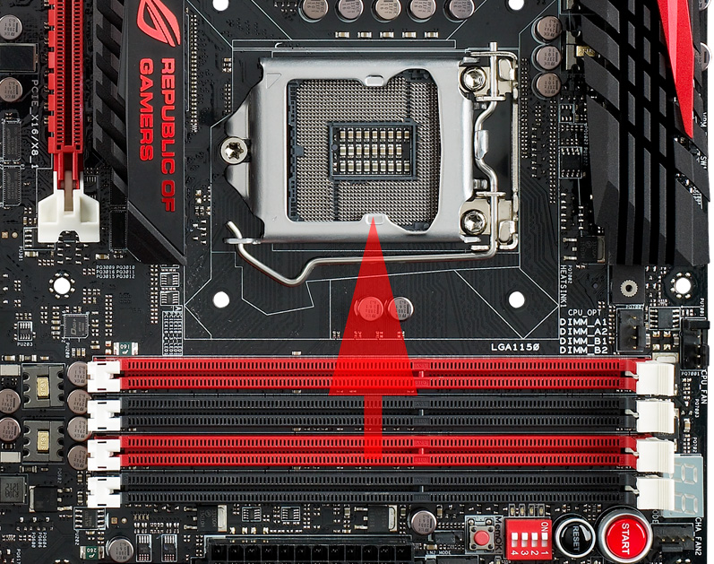
Оперативная память
При использовании двух модулей памяти устанавливайте их в красные слоты (расположены ближе к процессору).
iGPU (встроенное графическое ядро)
Встроенное графическое ядро при работе выделяет тепло. Логично, что при его отключении вы можете добиться лучших результатов разгона. Используйте PCI-Express видеокарту и в BIOS отключите (Disabled) уфнкцию iGPU Multi-Monitor Support для отключения графического ядра.
Охлаждение процессора
Используйте только самые лучшие системы охлаждения, т.к. процессоры в исполнении LGA1150 несколько горячее, чем могли бы быть и при больших нагрузках возможно срабатывание защиты (Thermal Throttling). При разгоне строго рекомендуется использовать такие системы охлаждения, которые обдували бы радиаторы на подсистеме питания. Или же обеспечить их обдув другими вентиляторами.
Процессоры Haswell очень чувствительны к температуре. Чем лучше вы их охлаждаете, тем сильнее можете разогнать. Экспериментально доказано, что при отрицательных температурах результаты разгона впечатляют даже при разумных значениях напряжений. Если вы планируете собрать систему, например, с фреоновой системой охлаждения, то обязательно позаботьтесь о изоляции электронных компонентов от конденсата. Температуру процессора можете смотреть в утилите CoreTemp.
Теперь можно переходить к рекомендациям по настройке системы в BIOS.
UEFI BIOS
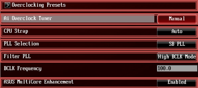
На Maximus VI Extreme предустановлено 5 профилей настроек разгона. Они могут стать основой для разгона вашего экземпляра процессора — надо будет только немного скорректировать параметры.
Установите параметр Ai Overclock Tuner в значение Manual, чтобы получить доступ к управлению BCLK. Можете установить режим X.M.P. для установки всех основных параметров оперативной памяти в соответствием с характеристиками, заявленными производителем. Данный режим также может быть выбран в качестве базового, затем его настройки могут быть скорректированы.
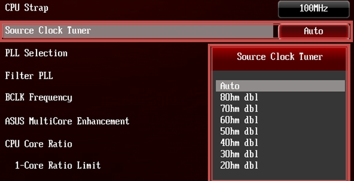
CPU Strap устанавливает разные значения страпов для процессора. Это позволит разогнать BCLK до максимально возможных для вашего процессора значений.
Связь между частотами BCLK, PCIE и DMI такая: PEG Frequency = DMI Controller Frequency = 100 x (BCLK / CPU Strap).
Помните, что для разных процессоров работоспособные страпы могут отличаться.
Опция Source Clock Tuner будет недоступна, если значение CPU Strap не установлена в фиксированное значение.
Параметр PLL Selection может быть установлен в режим Self Biased Mode (SB-PLL), что скажется на лучшем разгоне BCLK (базовой частоты), но может ухудшиться работа PCI-E 3.0 из-за возрастания фазового дрожания цифрового сигнала (джиттера) PCI-E. Пользователь может установить режим Inductance/Capacitance Mode (SB-LC), чтобы минимизировать джиттер PCI-E для лучшей совместимости с PCI-E 3.0 устройствами.
Параметр Filter PLL может быть установлен в режим High BCLK Mode для достижения высоких значений BCLK, но это грозит увеличением джиттера. Такой режим работы обычно требуется, чтобы установить BCLK свыше 170 МГц. Если вам не нужны такие значения, то смело ставьте режим Low BCLK Mode.
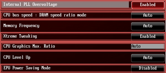
ASUS MultiCore Enhancement надо включить (Enabled), чтобы система автоматически поднимала частоту процессора до максимального значения в соответствии с вашими настройками, когда они превышают стандартные значения.
Internal PLL Overvoltage надо включить (Enabled) для наибольшего разгона по множителю. Но также помните, что работа S3/S4 может приводить к невозможности работы некоторых модулей оперативной памяти.
Параметр CPU bus speed: DRAM speed ratio может быть установлен 100:100 или 100:133. Выбор одного из эти соотношений может быть полезным для установки точной частоты оперативной памяти. При соотношении частот DMI/PEG 1:1, при увеличении частоты DMI/PEG на 1%, частота памяти увеличится также на 1%.
Включение Xtreme Tweaking может добиться увеличения производительности в старых бенчмарках.
CPU Graphics Max. Ratio рекомендуется ставить на минимально возможное значение (25), чтобы встроенное графическое ядро не потребляло много энергии и не выделяло много тепла.
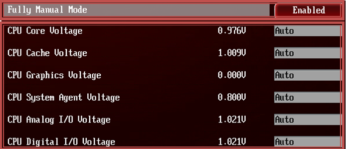
EPU Power Saving Mode рекомендуется выключить (Disabled), чтобы система не сбрасывала частоты и напряжения в режиме простоя.
Fully Manual Mode — эксклюзивный режим от ASUS, благодаря которому можно вручную настроить шесть ключевых напряжений на процессор. В этом режиме процессор не снизит ни одно из шести напряжений во время простоя, даже если включены EIST или C-States. Если вам нужно энергосбережение, то надо выключить эту опцию.
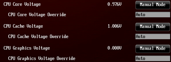
Три наиболее важных напряжения CPU Core Voltage, CPU Graphics Voltage, CPU Cache Voltage можно установить в режим ручной настройки (Manual), чтобы стали доступны опции CPU Core Voltage Override, CPU Graphics Voltage Override и CPU Cache Voltage Override. В этом режиме работы внутренний регулятор напряжений подаёт точное напряжение на CPU Vcore, CPU Graphics и CPU Cache. Этот режим начнёт работать как только значения Voltage Override превысят значения Auto. В этом режиме напряжения во время простоя не снизятся, даже если включены EIST или C-States.
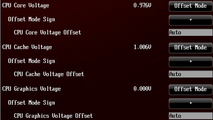
Параметр Offset Mode открывает режим Offset Mode Sign для изменения напряжений CPU Core Voltage Offset, CPU Graphics Voltage Offset и CPU Cache Voltage Offset. Чтобы установить уровень смещения напряжения, изменяйте эти параметры. Режим Auto представляет собой настройку от профессиональных инженеров ASUS. Если изменить напряжение на минимальный шаг +-0.001 В, то вы получите напряжение по умолчанию.
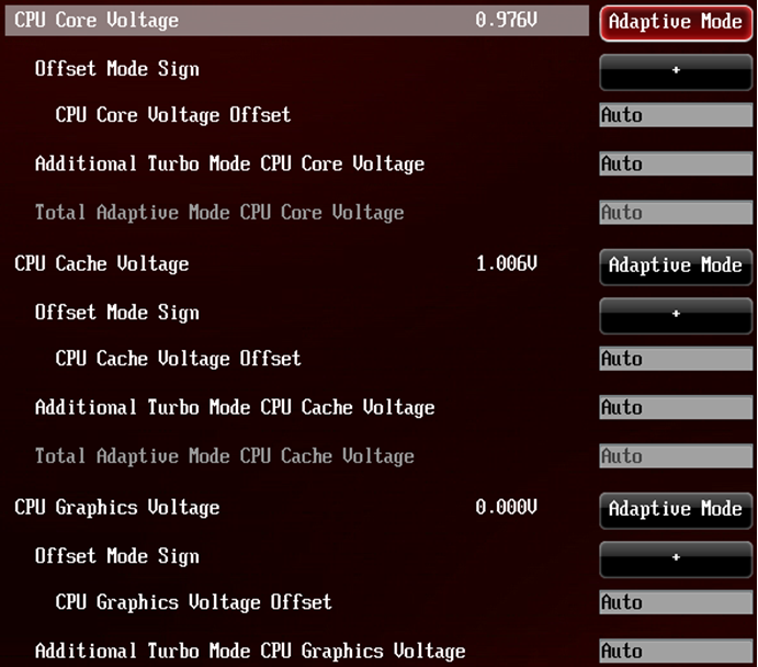
В режиме Adaptive Mode будет доступен режим Offset Mode и дополнительный режим Additional Turbo Mode Voltage для CPU Vcore, CPU Graphics и CPU Cache. Адаптивный режим можно считать расширением оффсетного режима. Дополнительно заданное напряжение будет активно во время работы Turbo Boost. Режим Auto представляет собой настройку от профессиональных инженеров ASUS. Если изменить напряжение на минимальный шаг +-0.001 В, то вы получите напряжение по умолчанию.

Отключение функции SVID Support прекращает взаимодействие процессора с внешним регулятором напряжения. При разгоне рекомендуется значение Disabled.
Разделение напряжений на Initial CPU Input Voltage и Eventual CPU Input Voltage позволятее более точно задать напряжения до и после прохождения POST. Это позвляет «неудачным» процессорам пройти POST с более высоким напряжением и снизить его для дальнейшей работы.

CPU Spread Spectrum надо выключать (Disabled) при разгоне процессора.
BCLK Recovery надо включить (Enabled) при разгоне процессора, чтобы система могла загрузиться в BIOS в безопасном режиме при некорректно выставленных настройках частоты.
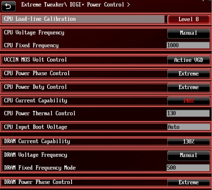
CPU Load-Line Calibration можно установить на максимальный уровень (8) для того, чтобы напряжение не проседало при нагрузке на процессор в разгоне. Уровень можно снизить для снижения энергопотребления и тепловыделения, если система остаётся стабильной.
Параметр CPU Voltage Frequency может быть установлен в режим «Manual», чтобы выбрать фиксированную частоту. Чем выше частота, тем стабильнее входное напряжение (CPU Input Voltage). Увеличение этой частоты может дать увеличение разгона BCLK, но всё зависит от экземпляра процессора (некоторым может требоваться меньшая частота для больших значений BCLK). Настоятельно рекомендуется включить Enable VRM Spread Spectrum или Enable Active Frequency Mode, если вы не намерены устанавливать фиксированное значение частоты процессора.
VCCIN MOS Volt Control можно увеличить для повышения стабильности, но и нагрев будет усиливаться. Если выставить значение Active VGD, то VCCIN MOS Volt Control будет динамически подстраиваться в зависимости от загрузки процессора.
CPU Power Phase Control надо установить в значение Extreme, чтобы были активны все фазы. Иначе во время простоя некоторые фазы неактивны. Это может позволить увеличить разгон по частоте.
CPU Power Duty Control надо установить в значение Extreme. В таком режиме предпочтение отдаётся подаче напряжения на iVR, а не балансу с температурой. В таком режиме можно получить чуть больший разгон.
CPU Current Capability устанавливаем 140%, чтобы сдвинуть порог срабатывания защиты от перегрузки по току. Это позволит увеличить разгон.
Значение CPU Power Thermal Control можно увеличить, если у вас проблемы с перегревом питания. Но настоятельно рекомендуется не изменять данный параметр. Если у вас проблемы из-за перегрева, то лучше поставить дополнительное охлаждение на радиатор подсистемы питания.
CPU Input Boot Voltage — начальное напряжение от подсистемы питания (Extreme Engine DIGI+ III) на интегрированный контроллер напряжений (FIVR — Fully Integrated Voltage Regulator), которое используется до того, как загружается BIOS. Это напряжение активно до того, как применяется напряжение Initial CPU Input Voltage, заданное из Extreme Tweaker. Тщательный подбор данного напряжения может помочь в достижении максимальной частоты процессора.
CPU Current Capability в значении 130% сдвигает порог срабатывания защиты от перегрузки по току для DRAM VRM. Способствует увеличению разгона оперативной памяти.
DRAM Voltage Frequency в Manual позволяет вручную настроить частоту VRM. Чем выше частота, тем стабильнее напряжение vDDR, что позволит добиться большего разгона памяти (не забываем, что для каждой планки разгон разный).
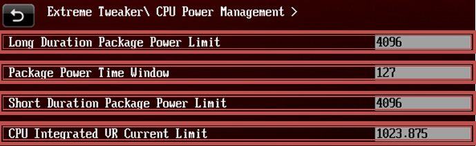
DRAM Power Phase Control в значении Extreme не допускает отключения фаз питания памяти. Это может позволить увеличить разгон памяти или увеличить стабильность работы, если модули памяти установлены во всех слотах.
Long Duration Packet Power Limit определяет максимальное значение для срабатывания троттлинга когда потребляемая мощность превышает определенный уровень. Можно сказать, что это первый уровень защиты процессора от повреждения. По умолчанию, это значение TDP от Intel. Если оставить в режиме «Auto», то будет установлено значение, рекомендуемое экспертами ASUS (OC Expert Team).
Package Power Time Window — значение в секундах, которое указывает сколько процессору дозволено работать с превышением TDP (то значение, которое мы задали в Long Duration Package Power Limit). Максимально возможное значение — 127.
Short Duration Package Power Limit указывает максимально возможное потребление энергии при очень кратковременных нагрузках, чтобы избежать нестабильности системы. Это можно считать вторым уровнем защиты процессора. Intel считает нормальным значение 1.25 от Long Duration Package Power Limit. Хотя по спецификации Intel для срабатывания Short Duration Package Power Limit кратковременные нагрузки могут быть не более 10 мс, материнские платы ASUS могут выдерживать гораздо большее время.
CPU Integrated VR Current Limit определяет максимальный ток от CPU Integrated Voltage Regulator при экстремально высоких нагрузках. Максимальное значение 1023.875 по сути отключает снятие лимита для iVR, который отключает троттлинг из-за превышения стандартных параметров тока при разгоне.
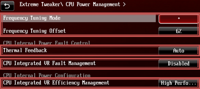
Frequency Tuning Mode определяет скорость работы процессора с iVR. Значение +6% обеспечит более стабильную подачу всех шести основных напряжений. Снижение этого параметра может снизить температуру на несколько градусов.
Thermal Feedback определяет будет ли процессор троттлить при перегреве внешней подсистемы питания. Эта настройка определяет будет ли работать защита от перегрева подсистемы питания. Если отключаете эту защиту, то настоятельно рекомендуется контроллировать температуру радиатора.
CPU Integrated VR Fault Management рекомендуется выключить, если повышаете напряжение вручную. Отключение может быть полезно при разгоне.
CPU Integrated VR Efficiency Management рекомендуется установить в режим High Performance, чтобы увеличить разгонный потенциал. Режим Balanced принесёт небольшую экономию энергии.
Power Decay Mode отвечает за энергосбережение в простое. При разгоне рекомендуется выключать (Disabled).
Idle Power-in Response при разгоне рекомендуется устанавливать в режим Regular. Режим Fast устанавливается для снижения энергопотребления.
Idle Power-out Response при разгоне рекомендуется устанавливать в режим Fast, что позволяет подавать на процессор чуть более высокое напряжение с наименьшими задержками.
Параметр Power Current Slope при значении LEVEL-4 сдвигает время троттлинга чуть дальше.
Power Current Offset определяет смещение параметра Power Current Slope. Значение -100% сдвигает время троттлинга процессора.
Power Fast Ramp Response определяет насколько быстро должен реагировать iVR на запрос напряжение процессором. Чем выше значение, тем быстрее будет реакция. Можно установить значение 1.5 для улучшения разгона.
Power Saving Level 1 Threshold определяет минимальный уровень энергопотребления, когда процессор должен запустить троттлинг. Установите 0 для отключения этой функции.
Power Saving Level 2 Threshold — аналогично пункту выше.
Power Saving Level 3 Threshold — аналогично пункту выше.
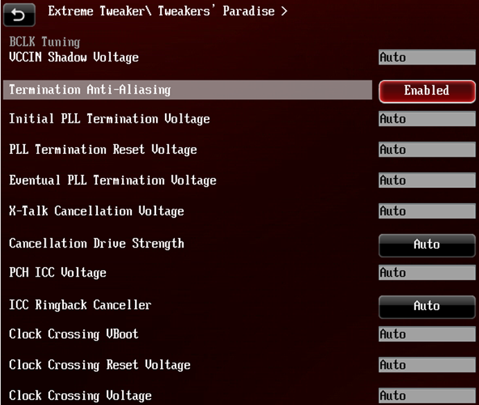
VCCIN Shadow Voltage — напряжение, которое подаётся от внешней подсистемы питания на внутренний контроллер питания во время прохождения POST. Это напряжение активно между CPU Input Voltage и Eventual CPU Input voltage. В режиме Auto напряжение будет задано автоматически, не выше и не ниже безопасных порогов.
Termination Anti-Aliasing рекомендуется включить (Enabled) для улучшения разгона.
PLL Termination Voltage (Initial / Reset / Eventual) рекомендуется менять при экстремальном разгоне при отрицательных температурах. Номинальное значение 1.2 В. Безопасные напряжения — до 1.25 В и выше 1.6 В. Не устанавливайте напряжение между 1.25 В и напряжением iVR, чтобы избежать быстрой деградации процессора.
При разгоне BCLK свыше 160 Мгц не забывайте настроить напряжения PLL Termination Reset Voltage и Eventual PLL Termination Voltage на одинаковый уровень с Eventual CPU Input Voltage или выше. Например, если Eventual CPU Input Voltage равно 1.9 В, то PLL Termination Reset Voltage и Eventual PLL Termination Voltage должны быть 1.9 В или выше для достижения оптимального эффекта.
Если вы не планируете разгонять BCLK свыше 160 МГц, то PLL Termination Voltage надо снизить до 1.1 или 1.0 В. Проще говоря, установите это значение до 1.25 В или на равне с CPU Input Voltage для достижения оптимального результата.
X-Talk Cancellation Voltage можно увеличить, если система работает нестабильно (например, BSOD 0124). Но эффект будет противоположным, если Max. Vcore Voltage работает под режимом LN2 — в этом случае уменьшение напряжение увеличит стабильность. По умолчанию — 1.00 В.
Cancellation Drive Strength управляет режимом работы X-Talk Cancellation Voltage.
PCH ICC Voltage — напряжение на интегрированный генератор тактов. По умолчанию — 1.2 В.
Для высокой частоты DMI (>=115 МГц) — пробуйте 1.2500 В или ниже.
Для низкой частоты DMI ( = 120 МГц).
DMI De-emphasis Control можно изменить вручную для лучшего разгона DMI. Но значение +6 является оптимальным.
Параметр SATA Drive Strength может быть настроен вручную для улучшения стабильности работы SATA. По умолчанию — 0. Можно пробовать менять в обе стороны.
CPU PCIE Controller в режиме Disabled отключает встроенный в процессор PCIEx16 контроллер для увеличения производительности в 2D бенчмарках. В таком случае рабочим остаётся только слот PCIE_x4_1.
GEN3 Preset в режиме Auto является оптимальным значением. Но можете попробовать все три предустановленных профиля и выбрать самый производительный. Особенно это полезно при тестировании конфигураций SLI или CrossFireX.
PLX 0.9V Core Voltage / PLX 1.8V AUX Voltage — управление напряжением на PLX PEX8747 (мост PCIE 3.0).
PCIE Clock Amplitude можете настроить вручную, подобрав наилучший режим при высокой частоте PCIe (из-за высокой частоты BCLK). Чаще всего, выше — лучше.
Internal Graphics (встроенное графиеское ядро) желательно отключить для улучшения разгона.
Рекомендуется отключить все неиспользуемые устройства и контроллеры для увеличения стабильности системы в разгона и вообще для достижения наилучших результатов.
Некоторые параметры рекомендуется оставлять в режиме Auto, доверившись профессионалам из команды ASUS.
Данная статья является вольным переводом официальной статьи ASUS ROG.
Если вы нашли какую-либо неточность, то сообщите об этом в официальном сообществе ASUS Republic of Gamers (ROG) Россия или GreenTech Reviews.
Руководство по разгону процессоров Intel Broadwell-E
Разгон многоядерных процессоров семейства Broadwell-E — задача крайне непростая, а все потому, что эти монстры внушительных размеров (CPU для Socket LGA 2066 гораздо больше в плане габаритов, нежели камни для LGA 115x) выделяют огромный объем тепла даже в номинале. Для достижения высоких тактовых частот понадобится мощное охлаждение (желательно жидкостное). И это первое, о чем стоит позаботиться на стадии подготовки к оверклокингу ЦП из указанной линейки.
Для разгона Core i7-6950X необходима кастомная СВО с трехсекционным радиатором.
Предлагаем обратить внимание на опубликованную ниже таблицу. В ней отображены режимы работы ЦП Core i7-6950X с той или иной СО. От выбора системы охлаждения зависит не только стабильная тактовая частота и минимально допустимый вольтаж на ядре, но и успешное прохождение стресс-тестов. Могучего двухвентиляторного кулера Noctua NH-D15 порой недостаточно даже для легкого разгона Core i7-6950X. Здесь нужна хорошая вода.
Эффективное охлаждение центрального процессора, как уже было сказано выше, положительным образом сказывается на температурных показателях, стабильной работе ПК и значении Vcore (чем ниже градусы, тем меньший вольтаж требуется для работы ЦП без сбоев).
| Тактовая частота | Вольтаж | Температура | Охлаждение | Стабильность |
|---|---|---|---|---|
| 4300 МГц | 1,25 В | 55 градусов | Кастомная «вода» с тройным радиатором | Да (часовой стресс-тест пройден) |
| 4300 МГц | 1,25 В | 65 градусов | AIO (тройной радиатор) | Нет (вылет после 30 минут) |
| 4300 МГц | 1,275 В | 68 градусов | AIO (тройной радиатор) | Да (часовой стресс-тест пройден) |
| 4300 МГц | 1,275 В | 85 градусов | Noctua NH-D15 | Нет (вылет после 2 минут) |
| 4300 МГц | 1,3 В | 91 градусов | Noctua NH-D15 | Нет (вылет после 2 минут) |
Если коротко, то для разгона Core i7-6950X необходима кастомная СВО с трехсекционным радиатором, а не вариант формата AIO (все в одном).
Во время оверклокинга важно отводить тепло не только от ЦП, но и от подсистемы питания материнской платы. Если вы планируете разогнать тот же самый Core i7-6950X выше 4 ГГц, позаботьтесь об установке вентилятора на VRM системной основы.
Материнские платы с чипсетом Intel X99, совместимые с процессорами Broadwell-E, оснащены 8-контактным разъемом EPS 12V и дополнительным 4-контактным коннектором. Оба должны использоваться при разгоне. Если задействован только 8-pin коннектор, может сработать система защиты от перегрузки по току.
Если в вашем распоряжении есть только 8-контактный разъем, убедитесь, что блок питания способен подавать ток свыше 30А на линию EPS 12V.
Статистика разгона
По статистике, только 20% процессоров семейства Broadwell-E способны функционировать на 4,4 ГГц (1,38 В). Более 75% устройств на том же самом вольтаже стабильны на 4,3 ГГц. И лишь 5% CPU запустятся на 4200 МГц, если напряжение на ядре не превышает 1,35 В.
Обратите внимание на максимальные показатели Vcore, которые мы использовали для разгона процессоров Core i7-6850K, Core i7-6800K, Core i7-6900K и Core i7-6950X (во всех случаях применялась мощная система жидкостного охлаждения). Цифры приведены в таблице ниже.
| Процессор | Максимальный вольтаж с использованием «воды» |
|---|---|
| Core i7-6950X | 1,225 В Prime95 1,38 В Handbrake |
| Core i7-6900K | 1,275 В Prime95 1,43 В Handbrake |
| Core i7-6850K и i7-6800K | 1,33 В Prime95 1,47 В Handbrake |
Если вы планируете использовать воздушное охлаждение, то от указанных показателей Vcore необходимо отнять 0,1 В или более (в зависимости от температуры окружающей среды и возможностей используемого кулера).
Про разгон оперативной памяти
Номинально процессоры семейства Broadwell-E совместимы с оперативной памятью DDR4-2400. Любая более высокая тактовая частота (даже применительно к профилям XMP) классифицируется как разгон. Для сравнения, официальная поддержка Haswell-E ограничена стандартом DDR4-2133.
Параметры System Agent (VCCSA) и IO (VCCIO) являются основными для разгона контроллера памяти.
Оптимальная производительность системы, в которой установлен процессор Broadwell-E, зафиксирована при использовании ОЗУ стандарта DDR4-3200, но имейте в виду, что крайне редко четырехканальные наборы памяти хорошо разгоняются. Вам вряд ли удастся завести четыре планки с номиналом DDR4-2400 на 3200 МГц. За хорошие и шустрые модули придется заплатить.
Оптимальным вариантом для пользователей, которые не желают выходить за рамки разумного бюджета, являются наборы стандарта DDR4-2400-3000. Не забывайте и о том, что важно использовать модули, входящие в единый комплект.
Установка различных планок (даже если они одной марки и модели) в систему негативным образом скажется на итогах оверклокинга. Хотя бывают и исключения.
Мы не наблюдали каких-либо негативных последствий, связанных со стабильной работой памяти при разгоне процессора. По большей части ограничения частоты ядра ЦП не зависят от скоростей памяти вплоть до частоты DDR4-3200.
Параметры System Agent (VCCSA) и IO (VCCIO) являются основными для разгона контроллера памяти. При настройке вручную увеличивайте или уменьшайте вольтаж постепенно. Подача слишком высокого напряжения может отрицательно сказаться на стабильной работе ПК, ровно как и недостаточное.
Максимальное напряжение, которое мы используем при ручной настройке этих параметров, составляет 1,30 В. Для скоростей памяти ниже DDR4-3000 достаточно 1,20 В.
Увеличение частоты Uncore
По сравнению с Haswell-E, у семейства Broadwell-E с разгоном функционала Uncore все не так гладко. При стандартных методах охлаждения самая высокая стабильная частота, с которой справляется большинство процессоров, ограничена 3,8 ГГц. ЦП Haswell-E способны работать на частоте выше 4,2 ГГц, а лучшие — на частоте выше 4,6 ГГц.
Есть также несколько побочных эффектов разгона Uncore, о которых нужно помнить. Мы включили несколько снимков осциллографа ниже, показывающих изменения энергопотребления из-за увеличения напряжения и частоты Uncore. Потребляемый ток EPS 12V показан в верхнем левом углу каждого снимка экрана.
При частоте ядра ЦП 4,3 ГГц и частоте Uncore по умолчанию энергопотребление составляет около 200 Вт.
Разгон Uncore до 3,7 ГГц при вольтаже 1,30 В приводит к увеличению энергопотребления на 30 Вт и скачку температуры на пять градусов при полной нагрузке процессора.
Поскольку прирост производительности от разгона Uncore ограничен отдельными рабочими нагрузками, в некоторых случаях имеет смысл оставить этот пункт с настройками по умолчанию с точки зрения энергопотребления и температуры.
Максимальное напряжение, которое мы используем для ручной настройки Uncore, составляет 1,35 В. Все, что выше, приводит к экспоненциальному росту энергопотребления.
Регулируемые настройки в UEFI BIOS
Ai Overclock Tuner: установите значение Manual, если хотите настроить BCLK вручную. После перехода в ручной режим появятся настройки CPU Strap, Source Clock Tuner, PLL Selection, Filter PLL, BCLK Frequency и Initial BCLK Frequency.
CPU Strap: изменяет эталонную тактовую частоту для ЦП и памяти. Значение по умолчанию составляет 100 МГц. Если используется множитель процессора, равный х44, рабочая частота составит 4400 МГц. Если выставить для CPU Strap 125 МГц и множитель х44, получим 5500 МГц (44х125). Предпочтительнее использовать номинальный вариант (100 МГц).
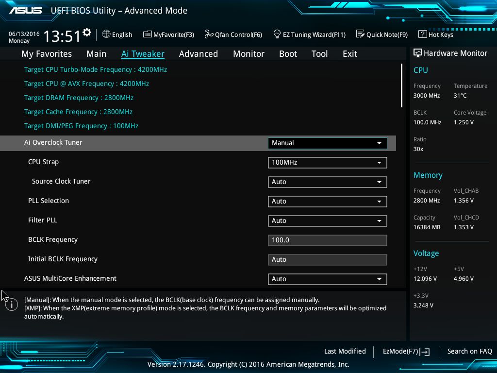
Source Clock Tuner: этот параметр изменяет частоту шины DMI, чтобы она оставалась стабильной при изменении BCLK. Его можно оставить в положении Auto, если вы не планируете экспериментировать с высокими значениями BCLK.
PLL Selection: режим LC PLL предпочтительнее для значения 100 МГц применительно к параметру CPU Strap и BCLK по умолчанию. Вариант SB стоит выбрать, если вы планируете менять базовое значение BCLK. Для обычного использования оставляем режим Auto.
По сравнению с Haswell-E, у семейства Broadwell-E с разгоном функционала Uncore все не так гладко.
Filter PLL: может использоваться для увеличения стабильной работы процессора и памяти при изменении BCLK. Выберите соответствующую настройку High или Low BCLK в соответствии с используемой частотой BCLK.
BCLK Frequency: BCLK — это эталонная тактовая частота для ЦП, шины Uncore, памяти, шин PCIe и DMI. Любые изменения BCLK влияют на указанные шины. Обычно изменения BCLK не требуются для системы, которая используется в качестве рабочей станции или игровой машины. Единственными исключениями из этого правила являются ситуации, когда соотношение DRAM требует небольшого изменения BCLK для получения правильной частоты памяти.
Если необходимо внести изменения вручную, не изменяйте показатель BCLK более, чем на +/- 3 МГц от частоты по умолчанию.
Initial BCLK Frequency: значение BCLK, которое используется при прохождении POST. По умолчанию установлено то же значение, что и частота BCLK. Изменения могут быть полезны в ситуациях, когда система работает стабильно в операционной системе, но не при прохождении POST. Изменение этого показателя на 5 МГц в сторону понижения (относительно частоты BCLK) может помочь последовательно пройти POST.
После корректировки Initial BCLK Frequency все шины заведутся на указанной частоте. Это может повлиять на общую стабильность работы ОС. Поэтому этот вариант следует использовать только в крайнем случае, когда изменения напряжения и таймингов памяти не помогают.
ASUS Multicore Enhancement: при выборе значения Auto коэффициент Turbo применяется ко всем ядрам. Действует только при стандартных настройках ЦП. При ручном разгоне коэффициенты Turbo назначаются в соответствии с настройками соотношения ядер ЦП.
CPU Core Ratio: существует три варианта настройки указанной опции:
- Sync all cores: все ядра будут функционировать на выбранном значении.
- By Core Usage: позволяет независимо применять тот или иной коэффициент к каждому ядру (настраивается вручную с помощью диспетчера задач Windows).
- By Specific Core: этот параметр работает в паре с технологией Intel Turbo Boost Max Technology 3.0. Опция автоматически определяет, какое ядро имеет лучший частотный потенциал, и помечает его как любимое ядро (звездочка в UEFI). По умолчанию драйвер Turbo Boost 3.0 назначает однопоточные рабочие нагрузки любимому или самому быстрому ядру.
Мы рекомендуем использовать параметр Sync all cores вместе с опцией ASUS Thermal Control Tool, чтобы получить максимальную производительность от архитектуры Broadwell-E. Параметры By Core Usage и By Specific Core имеют явные ограничения, которые сводят на нет их преимущества при разгоне системы.
AVX Instruction Core Ratio Negative Offset: этот параметр снижает частоту ядра ЦП на применяемое значение при выполнении рабочей нагрузки с использованием инструкций AVX. Нагрузка на ЦП при запуске профильных задач (с AVX) значительно выше, чем без AVX, поэтому и был введен данный параметр.
Min CPU Cache Ratio: устанавливает минимальное значение множителя Uncore. Минимальное соотношение активно, когда ЦП находится в состоянии пониженного энергопотребления.
Во время оверклокинга важно отводить тепло не только от ЦП, но и от подсистемы питания материнской платы.
Max CPU Cache Ratio: устанавливает максимальное значение множителя Uncore. Максимальный коэффициент активен, когда ЦП загружен. Частота кэша (Uncore) определяется путем умножения BCLK на коэффициент кэша. Целевая частота отображается в левом верхнем углу страницы Ai Tweaker.
Internal PLL Overvoltage: увеличивает внутреннее напряжение PLL для лучшего разгона ЦП, однако мы не обнаружили, что этот параметр хоть как-то влияет на результаты оверклокинга.
BCLK Frequency: DRAM Frequency Ratio: отношение частоты DRAM к BCLK. Для обычного использования эту настройку можно оставить в режиме Auto, так как автоматически будет выбрано наилучшее соотношение в соответствии с выбранной пользователем частотой DRAM.
TPU: предустановленный разгон. Есть два варианта: для ПК с воздушным охлаждением и с жидкостным. Предпочтительнее использовать автоматическую настройку 5-Way Optimization, а не полагаться на указанные профили. Программное обеспечение 5-Way Optimization адаптирует разгон в соответствии с возможностями компонентов системы.
EPU Power Saving Mode: применяет различные протоколы энергосбережения для снижения энергопотребления системы. Этот параметр следует использовать только на штатных частотах процессора. Мы не рекомендуем использовать его при разгоне системы.
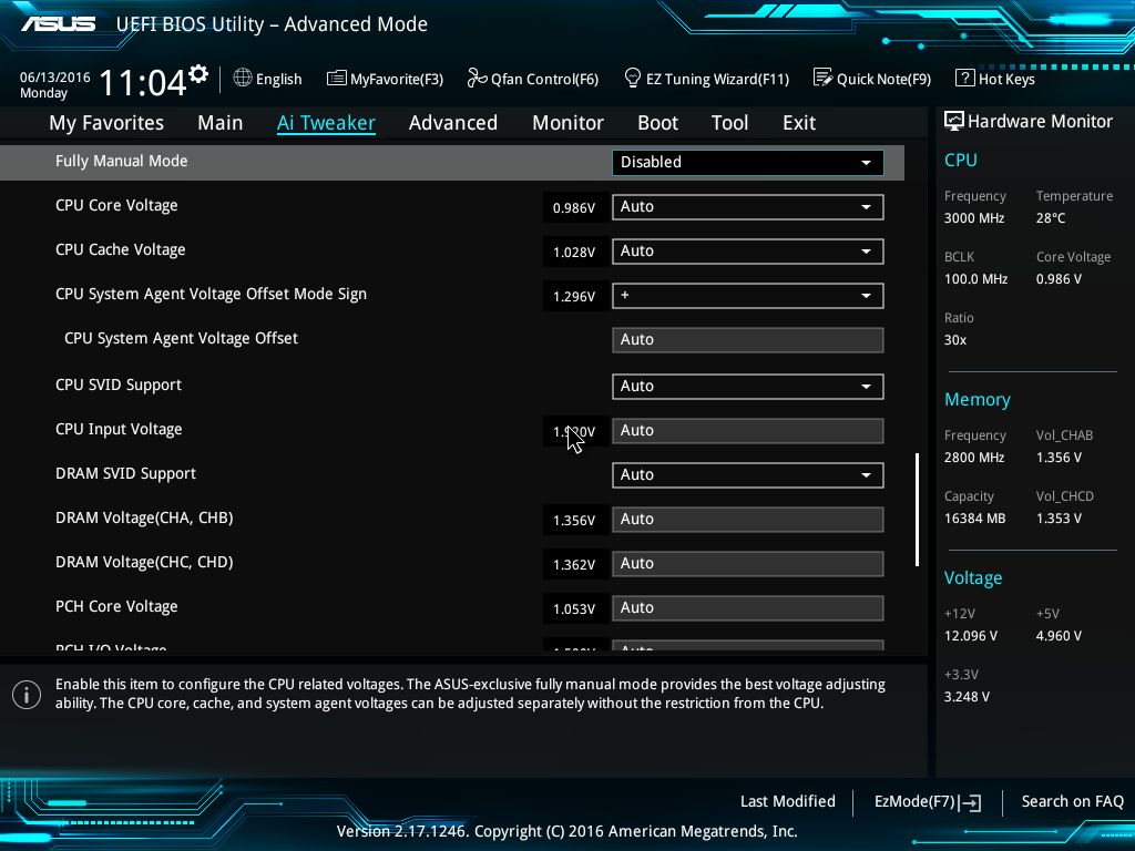
Fully Manual Mode: если этот параметр включен, доступны более высокие показатели напряжения, а вольтаж System Agent можно настроить в ручном режиме.
CPU Core Voltage: устанавливает режим управления напряжением на CPU (Vcore):
- Manual Mode: позволяет установить единое Vcore значение, которое применяется независимо от нагрузки.
- Offset Mode: в этом режиме мы можем добавлять или вычитать вольтаж из напряжения ЦП по умолчанию. Напряжение по умолчанию масштабируется в соответствии с активным коэффициентом множителя. Это обеспечивает экономию энергии. Побочным эффектом использования Offset Mode является то, что любое выбранное значение смещения будет применяться ко всем ядрам. Это может привести к нестабильной работе ПК.
- Adaptive Mode: адаптивный режим был разработан с учетом минусов режима Offset Mode. Он используется, когда процессор сталкивается с высокой нагрузкой. Преимуществом адаптивного режима является то, что он не изменяет напряжения для не-Turbo CPU коэффициентов.
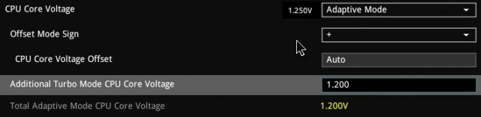
Чтобы использовать адаптивный режим, просто введите максимальное напряжение, которое вы хотите использовать при полной нагрузке ЦП (в поле «Additional Turbo Mode CPU Core Voltage»). Если вы хотите установить 1,20 В для полной нагрузки, просто введите 1,20. Целевое напряжение при полной нагрузке отображается в области Total Adaptive Mode CPU Core Voltage.
CPU Cache Voltage: устанавливает вольтаж для Uncore и имеет те же режимы напряжения, что и CPU Core Voltage. Если вы хотите отрегулировать напряжение кэш-памяти процессора, мы рекомендуем использовать ручной режим или Offset Mode, поскольку Adaptive Mode для Uncore не работает должным образом в режиме оверклокинга. Эта проблема микрокода Intel.
Для мониторинга частоты и температуры CPU используйте утилиты HWiNFO и AIDA64.
CPU System Agent: отвечает за обработку операций ввода-вывода между ЦП и другими устройствами. Вольтаж System Agent важен для разгона памяти. По умолчанию можно выбрать только Offset Mode. Чтобы получить доступ к ручному режиму, для параметра Fully Manual Mode выбираем Enabled.
Для скоростей памяти выше DDR4-3000 может потребоваться напряжение до 1,30 В. Некоторые процессоры имеют слабые контроллеры памяти, требующие повышенного вольтажа для стабильности. Если возможно, не переступайте порог в 1,30 В.
CPU SVID Support: эта функция обеспечивает связь между PCU (power control unit) процессора (блок управления питанием) и внешним регулятором напряжения для VCCIN. Это позволяет программному обеспечению считывать данные об энергопотреблении процессора. Роль SVID заключается в обеспечении связи между ЦП и встроенным регулятором напряжения (регулятор VCCIN) для энергосбережения.
CPU Input Voltage: обеспечивает входное напряжение 1,80 В для ЦП (постоянный ток). Все первичные внутренние шины напряжения регулируются этим источником вольтажа. Значение CPU Input Voltage должно быть как минимум на 0,45 В выше, чем CPU Vcore. В противном случае система может вести себя нестабильно. Максимальное напряжение, которое мы используем, составляет 1,95 В. Обратите внимание, что фактическое напряжение, подаваемое на ЦП, зависит от настройки LLC в меню внешнего управления питанием DIGI+.
DRAM SVID Support: связь между блоком управления питанием CPU и встроенными регуляторами напряжения DRAM. Роль SVID с точки зрения регулировки напряжения заключается в том, чтобы позволить ЦП связываться со встроенным регулятором напряжения DRAM (энергосбережение).
DRAM Voltage (CHA, CHB) и DRAM Voltage (CHA, CHB): вольтаж для модулей памяти.
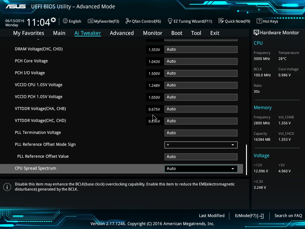
PCH Core Voltage: источник питания для PCH (platform controller hub). Этот параметр не требует настройки в процессе разгона.
PCH I/O Voltage: не нуждается в настройке, если шина DMI не разогнана.
VCCIO CPU 1.05V Voltage: для стабильной работы памяти данный параметр следует установить на значении 0,05 В меньше, чем System Agent Voltage.
VCCIO PCH 1.05V Voltage: не нуждается в регулировке, если шина DMI не разогнана.
VTTDRR: этот параметр следует оставить в режиме Auto.
PLL termination/PLL Reference/PLL Reference Offset Value: оставляем Auto. Регулировка этих параметров необходима лишь в случае экстремального разгона с применением жидкого азота.
CPU Spread Spectrum: оставляем Auto. Выбор Enable может отразиться на стабильности.
Методика тестирования
Прежде чем разгонять систему, запустите стресс-тесты со стандартными настройками. Часового прогона должно хватить. Убедитесь, что максимальная температура ЦП не выходит за рамки приличия и оставляет вам некоторый задел для оверклокерских экспериментов.
Следите за температурой, когда процессор находится под полной нагрузкой в течение нескольких минут. Убедитесь, что он не снижает тактовую частоту из-за перегрева.
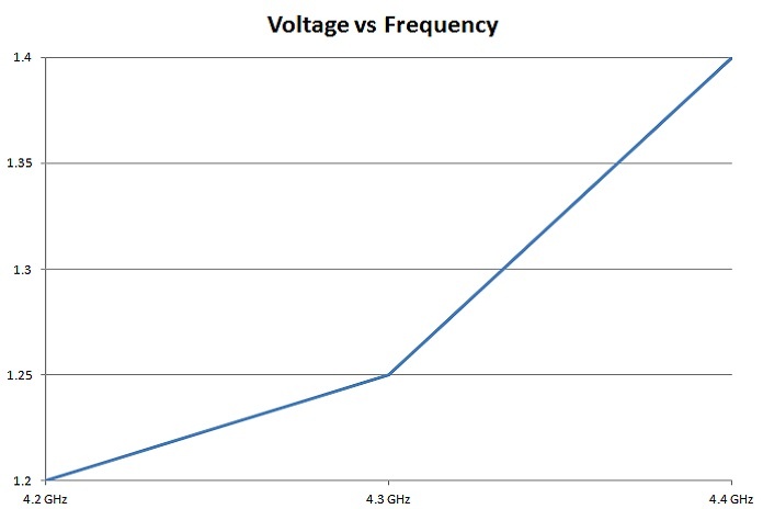
Для мониторинга частоты и температуры CPU используйте утилиты HWiNFO и AIDA64.
Если все в порядке, переходим к разгону. Сначала произведите оверклокинг только CPU, коэффициенты памяти и кэша не трогаем. Мы рекомендуем использовать режим адаптивного напряжения, а не ручной или Offset Mode. Для проверки стабильности работы ПК запускайте тест Cinebench R23.
Как только найдете стабильную тактовую частоту CPU, активируйте профиль XMP для модулей памяти и запустите стресс-тест с интенсивным использованием ОЗУ.
Если стабильность не может быть достигнута при включенном профиле XMP, попробуйте уменьшить тактовую частоту CPU. При этом оставьте Vcore на том же значении.
Если система стабильна при более низкой тактовой частоте ЦП, может потребоваться настройка напряжения Vcore, System Agent (VCCSA) и VCCIO. Если ни один из этих способов не помогает, поэкспериментируйте с таймингами памяти или напряжением DRAM.
Ниже опубликованы скриншоты конфигурации для разгона CPU до 4,2 ГГц с применением XMP: