Напряжение ШИМ ЦАП устанавливается за один период тактовых импульсов
Texas Instruments TL071A LF398-N OPA2277. CD74HC02
Широтно-импульсная модуляция (ШИМ) является лучшим способом преобразования для регулируемых источников постоянного напряжения с цифровым управлением, требующих высокой точности и разрешения. Изобретенный 50 лет назад [1, 2] метод ШИМ широко используется сегодня в импульсных источниках питания [3] и, в частности, в калибраторах постоянного тока [4, 5], позволяя достичь разрешения в 26 бит и линейности 0.2 ppm [6].
По сути, цифро-аналоговый преобразователь (ЦАП) на основе ШИМ устанавливает постоянную составляющую последовательности импульсов с фиксированным периодом и переменным коэффициентом заполнения. Теоретически постоянная составляющая такого сигнала определяется общим выражением ШИМ:
VP – амплитуда импульсов;
tP – длительность импульсов;
T – период сигнала.
Для ускорения процесса преобразования в современных ЦАП используются синхронные фильтры нижних частот, состоящие из интегратора и схемы выборки/хранения (S/H). В конце каждого периода напряжение интегратора запоминается в схеме S/H, и это напряжение является выходом всего преобразователя.
В некоторых преобразователях между выходом схемы S/H и интегратором включается резистор обратной связи. Чтобы получить быстрое и точное преобразование, надо две постоянные времени сделать равными периоду импульсов. В [2] четко сформулировано требование RF×C = T. Второе условие – RI×C = T – не обсуждается, но его легко найти, применив приведенное выше общее выражение ШИМ к их формуле (4).
Регулировка двух постоянных времени сводится к подбору емкости конденсатора интегратора С или периода T следования импульсов. Оба подхода связаны с определенными трудностями. Самое важное состоит в том, что нет никаких намеков на то, как выполнить эту регулировку автоматически.
В данной статье представлена схема и простая процедура, позволяющие заполнить этот пробел. Использование предлагаемого метода требует лишь одной регулировки. Вместо постоянной времени регулируется зарядный ток интегратора, что обеспечивает лучшее разрешение и линейность характеристики.
Концепция иллюстрируется Рисунком 1. Во время входного импульса ключ S разомкнут, и конденсатор интегратора заряжается двумя токами. Первый ток I1 = VP/R1 определяется импульсами ШИМ; он составляет 95% от номинального тока. Второй ток I2 задается дополнительным ЦАП. Он поставляет примерно 10% номинального тока, обеспечивая возможность подстройки скорости изменения напряжения интегратора в пределах ±5%. В конце импульса напряжение интегратора сохраняется в схеме S/H, после чего ключ S замыкается, и интегратор разряжается.
| Рисунок 1. |
Вспомогательный ЦАП обеспечивает диапазон регулировки ±5% для зарядного тока
интегратора; компаратор помогает микропроцессору подобрать правильный код ЦАП. |
Значение второго тока устанавливается путем записи соответствующего кода в регистр ЦАП. Каждый бит этого кода определяется отдельно с использованием метода последовательного приближения. Критерий регулировки основывается на выражении (1): при коэффициенте заполнения 50% выходное напряжение должно быть вдвое меньше амплитуды входных импульсов. Резисторы R3 и R4 и компаратор Cmp сообщают микропроцессору, насколько близко выходное напряжение к требуемому значению.
Схема представлена на Рисунке 2. Ее работа контролируется цепью синхронизации, построенной на логических элементах G1-G4, которая формирует импульсы управления для ключа сброса интегратора Q1 и внутреннего ключа устройства S/H.
| Рисунок 2. |
Полный набор оборудования включает в себя цепь синхронизации (G1-G4) для управления
работой интегратора и схемы S/H, усилитель (IC4a), повышающий чувствительность
компаратора и преобразователь уровня (Q2) для сопряжения выхода компаратора
с микроконтроллером. |
Как видно из временной диаграммы на Рисунке 3, по спадающему фронту сигнала ШИМ на выходе G4 устанавливается высокий уровень напряжения. Ключ сброса Q1 разомкнут, и интегратор формирует импульсы с отрицательным наклоном. По заднему фронту импульса ШИМ схема на элементах G1 и G2 формирует 10-микросекундный импульс для захвата напряжения интегратора схемой S/H. Элемент G3 суммирует импульсы VPWM и VG2, чтобы ключ сброса оставался разомкнутым, пока не будут завершены интегрирование и запоминание напряжения. По окончании импульса хранения ключ замыкается. Интегратор сбрасывается в ноль, ожидая следующего импульса ШИМ.
| Рисунок 3. |
Временные диаграммы в ключевых точках схемы для первых
двух циклов преобразования. |
В идеале, при амплитуде импульсов 5 В и коэффициенте заполнения 50% выходное напряжение должно быть равно –2.5 В. Калибровка начинается с конфигурирования системы ШИМ внутри микроконтроллера, чтобы установить частоту импульсов 1 кГц и коэффициент заполнения 50%. Затем микроконтроллер посылает в ЦАП код «100000000000» и ждет прерывания по заднему фронту импульса RstInt. По приходе заднего фронта микроконтроллер считывает выходной сигнал компаратора BitVal. Цепь R3-R4 и микросхема IC4 сравнивают VOUT с идеальным значением напряжения –2.5 В. Если напряжение VOUT более положительно, чем –2.5 В, выходной уровень компаратора равен 0, что означает, что первый бит в коде ЦАП должен измениться на 0; в противном случае этот бит сохраняет заданное значение 1. После этого микроконтроллер посылает в ЦАП код «x10000000000» и устанавливает значение второго бита в соответствии с реакцией компаратора. Далее посылается третье число «xx1000000000», и процесс продолжается до тех пор, пока не будут определены все 12 бит кода ЦАП.
Рисунок 4 демонстрирует процесс калибровки в действии. Желтый луч отмечает начало процедуры; это происходит на спадающем фронте импульса RstInt. Синий луч является выходным сигналом IC4a. Он «разбегается» в обе стороны от нулевого напряжения и постепенно сходится к нему. Нулевое значение обозначает выходное напряжение схемы S/H, составляющее половину амплитуды импульсов ШИМ. Реальное значение, измеренное цифровым мультиметром с разрешением 4.5 десятичных разряда, равнялось 0.49947. Использование профессионально изготовленной печатной платы и мультиметра с высоким разрешением, вероятно, позволит добиться лучшего соответствия.
| Рисунок 4. |
Метод последовательного приближения постепенно приводит выходной
сигнал к требуемому значению VP/2. |
По завершении калибровки микроконтроллер может изменить коэффициент заполнения сигнала ШИМ в соответствии с настройками пользователя. Поскольку скорость изменения напряжения интегратора уже установлена правильно, новое напряжение появится на выходе после всего лишь одного периода импульсной последовательности. Выходное напряжение будет в точности равно постоянной составляющей сигнала ШИМ, как это определяется теорией, и не будет иметь пульсаций. Самое замечательное, что откалибровать преобразователь можно в любое время и полностью автоматически.
Совет для профессионалов
Для достижения наилучшей точности настройки вместо общего источника питания +5 В используйте специальный источник напряжения. Обязательно проследите, чтобы отношение R3/R4 было максимально близким к 2:1, а напряжения смещения IC2 и IC4 были малы, насколько это возможно. Резисторы R1 и R2 должны быть металлопленочными с допусками 1%. Конденсатор C1 должен иметь точность не хуже 2% и низкий коэффициент диэлектрической абсорбции. Сопротивление открытого ключевого транзистора Q1 должно быть низким. Можно также использовать ЦАП с более высоким разрешением.
Самый совершенный в отрасли аудио операционный усилитель
Компания Texas Instruments (TI) представила аудио операционный усилитель (ОУ), устанавливающий новые стандарты качества звука. OPA1622 стал последним дополнением к линейке аудио микросхем компании, выпускаемых под брендом Burr-Brown и, фактически, является следующим поколением широкого распространенного ОУ OPA1612.

OPA1622 отдает в нагрузку мощность до 150 мВт и отличается сверхнизкими искажениями, уровень которых при выходной мощности 10 мВт составляет –135 дБ, что отвечает требованиям, предъявляемым к профессиональному аудио оборудованию. Небольшие размеры усилителя, экономичность и низкие искажения позволяют обеспечить высококачественное звучание таких портативных устройств, как усилители наушников, смартфоны, планшеты и USB аудио цифро-аналоговые преобразователи.
Ключевые особенности и преимущества операционных усилителей OPA1622:
- Раздвигает границы качества звука:
Разработчики усилителей для наушников получают прибор с низкими гармоническими искажениями, не превышающими –135 дБ при выходной мощности 10 мВт на нагрузке 32 Ом, что в 12 раз лучше, чем у ближайших конкурентов. Максимальная неискаженная выходная мощность 150 мВт при наименьших в отрасли шумах обеспечивает чистый путь прохождения сигнала для профессиональных аудио приложений.
- Оптимизирован для высококачественных портативных аудио устройств:
Миниатюрный компонент в безвыводном корпусе DFN площадью 3 x 3 мм потребляет 2.6 мА на канал и сохраняет высокую линейность выходного тока до уровня 80 мА с.к.з. Улучшенное подавление пульсаций питания (–97/–123 дБ на частоте 20 кГц) минимизирует влияние импульсных источников и позволяет, не ухудшая характеристик, исключить из схемы питания выходные LDO-регуляторы и сократить требуемую площадь печатной платы.
- Уникальное расположение выводов упрощает конструирование и снижает искажения:
Вывод разрешения микросхемы OPA1622 с привязанным к земле порогом переключения может без схем сдвига уровня напрямую управляться выходом общего назначения любого маломощного микроконтроллера. Инновационное расположение выводов улучшает топологию печатной платы и снижает уровень искажений при больших выходных мощностях.
- Устраняет слышимые щелчки и треск:
Исключительно эффективная схема управления ограничивает скачки выходного напряжения, когда OPA1622 переходит в режим отключения или выходит из него.
Созданная для OPA1622 SPICE-макромодель TINA-TI поможет конструкторам в соблюдении требований целостности сигналов на уровне печатной платы. В ближайшее время появятся примеры разработки прецизионных аудио ЦАП с выходами по напряжению, которые сократят время вывода на рынок усилителей для наушников, основанных на микросхеме OPA1622.
Техническая поддержка OPA1622 доступна в сообществе пользователей TI E2E и на форумах, где инженеры могут поискать готовые решения, получить помощь, поделиться знаниями и решить проблемы со своими коллегами и экспертами TI.
OPA1622 выпускается серийно в корпусе DFN размером 3 x 3 мм и поставляется партиями по 1,000 чипов.
Texas Instruments: OPA317 — операционный усилитель с малым напряжением смещения нуля и входными/выходными сигналами, равными напряжению питания (Rail-to-Rail)
 Семейство операционных CMOS-усилителей OPA317 обеспечивает высокую точность работы по самой конкурентной цене.
Устройства являются представителями серии усилителей Zerø-Drift, использующим фирменную технологию автокалибровки. Эта технология обеспечивает низкое напряжение смещения (90 мкВ макс.) и нестабильность тока покоя во времени и под влиянием температуры не более 35 мкА. Усилители семейства OPA317 способны работать с входными и выходными сигналами, равными напряжению питания, и имеют почти плоскую характеристику распределения шума. Работа усилителей гарантируется при напряжении питания не менее +1.8 В (±0.9 В) и не более +5.5 В (±2.75 В).
Устройства поставляются в различных корпусах, в зависимости от количества усилителей в одном корпусе. Так, одинарный усилитель OPA317 представлен в корпусах SC70-5, SOT23-5 и SOIC-8; сдвоенный OPA2317 – в корпусах MSOP-8 и SOIC-8; счетверённый OPA4317 – в корпусах SOIC-14 и TSSOP-14, а также VQFN-14. Диапазон рабочих температур всех усилителей составляет от –40°C до +125°C.
Отличительные особенности:
- Диапазон напряжения питания: от 1.8 В до 5.5 В
- Низкое напряжение смещения: 20 мкВ (тип.)
- Коэффициент подавления синфазного сигнала: 108 дБ (тип.)
- Ток покоя: 35 мкА (макс.)
- Граничная частота единичного усиления: 300 кГц
- Входные и выходные сигналы, равные напряжению питания (Rail-to-Rail)
- Встроенная система подавления электромагнитных и радиочастотных (EMI/RFI) искажений
- Диапазон рабочих температур: -40…+150°C
- Миниатюрные корпуса:
- Одинарный: SOT23-5, SC-70, SOIC-8
- Сдвоенный: MSOP-8, SOIC-8
- Счетверённый: SOIC-14, TSSOP-14
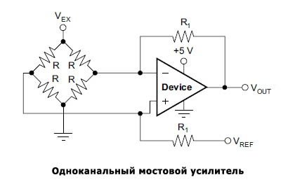 Область применения:
- Инструменты с аккумуляторным питанием
- Обработка сигналов с датчиков
- Электронные весы
- Медицинское оборудование
- Портативные тестеры
- Датчики тока, температуры
 Документация на операционные усилители серии OPA317 (англ.)
Op-Amps
At it’s most basic level, an operational amplifier (op-amp) is a discrete analogue integrated circuit which acts as a voltage-amplifier with very high gain.
An op-amp’s gain can be adjusted with the appropriate external circuitry (the op-amp’s internal gain does not change, but the gain of the entire circuit does). This is almost always done for any op-amp that is used as an amplifier. External circuitry can also manipulate the op-amp to act as as a current amplifier or perform “mathematical” operations on signals.
Schematic Symbol
An op-amp is commonly drawn on schematics as:
The basic schematic symbol for an op-amp.
You may see this symbol with or without the voltage supply pins \( +V_ \) and \( -V_ \) . If they are not present, it is assumed that they are connected up to a power source which should be obvious from the design intent.
- Buffers (a.k.a. voltage followers)
- Linear amplifiers, non-linear amplifiers
- Pre-amplifiers (amplifier’s with a input voltage of 10mV or less)
- Analogue mathematical operations (differentiators, integrators, summer, subtracters, e.t.c)
- Voltage to current (transconductance) and current to voltage conversions (transimpedance)
Op-Amp Topologies
Voltage Followers (a.k.a. Buffers)
A voltage follower (also known as a buffer) is one of the most basic circuits you can make with an op-amp.
An op-amp configured as a voltage follower (aka buffer).
The output voltage for a voltage follower is just simply:
As shown in Eq \(\ref\) , the output voltage is the same as the input voltage. Well isn’t this pointless? No, the key point to a voltage follower/buffer is that it can convert a high-impedance input into a low impedance output. Practically, this means that you can now sink/source more current from the output without the voltage changing. Buffers are great for boosting signals that travel across long distances, or for signals which get split and go to many devices (this is called fan-out, and is common with digital clock signals).
A simulation schematic for a voltage-follower op-amp is shown below.
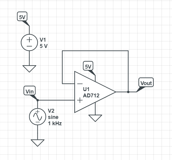
A simulation schematic for an op-amp configured as a voltage-follower (buffer).
The results of the simulation:
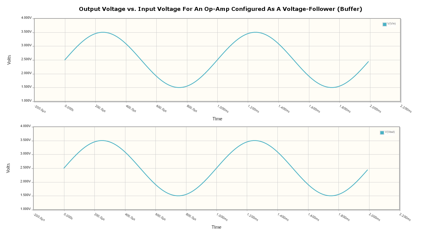
The simulation results for an op-amp configured as a voltage-follower (buffer). Note how the output voltage mirrors the input voltage exactly.
Non-Inverting Amplifiers
A op-amp in the non-inverting amplifier configuration is shown below.
An op-amp configured as a non-inverting amplifier.
The equation for the output voltage of the non-inverting amplifier is:
Notice the \(1\) in the gain equation? This means that no matter what you set the resistors \(R_f\) and \(R_i\) to, you can never get a gain which is less than one. This is one of the disadvantages of the non-inverting amplifier (you can have a gain of less than one with an inverting amplifier).
Simulation example for a non-inverting amplifier.
Here is a simulation schematic (circuit) for a non-inverting op-amp amplifier running from a single-ended supply. Because R1 ( \(R_f\) ) and R2 ( \(R_i\) ) are both \(1k\Omega\) , the op-amp has a voltage gain \(A_V\) of:
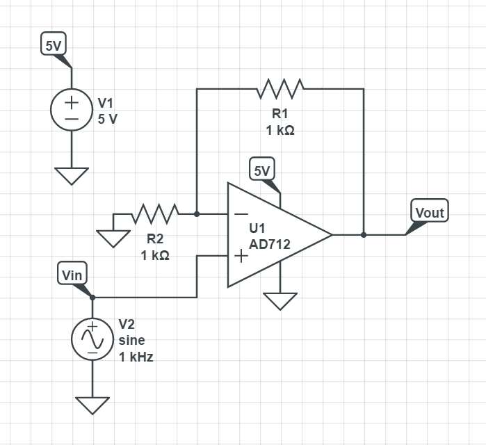
The simulation schematic for a non-inverting op-amp amplifier.
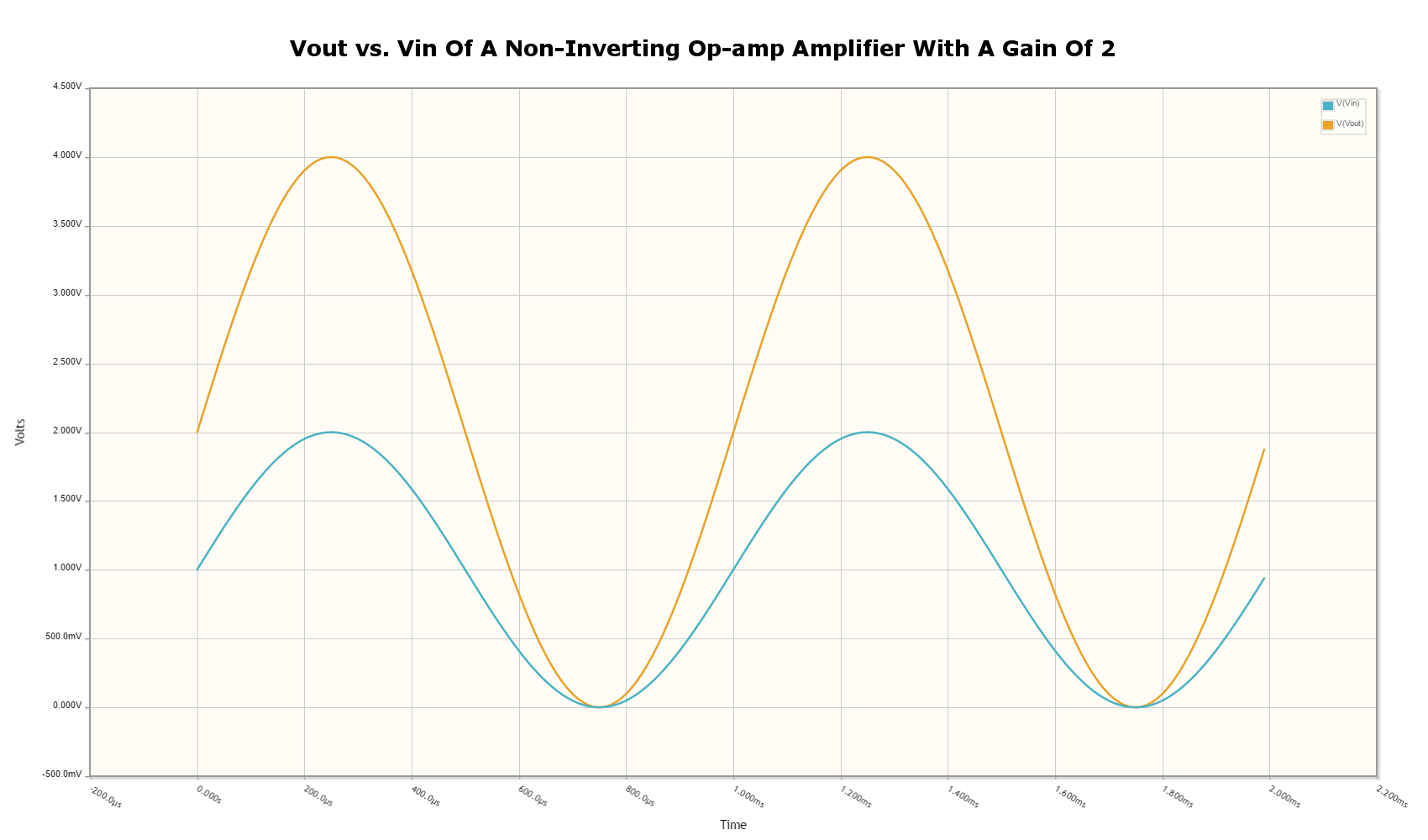
The results of the simulation are shown below. As you can see, the output voltage \(v_\) is exactly twice the input voltage \(v_\) .
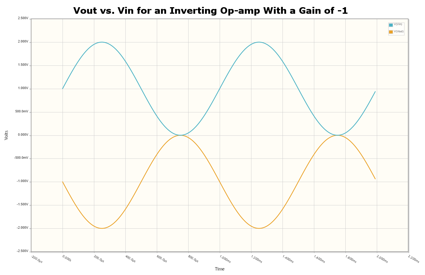
A schematic for simulating the behaviour of an inverting op-amp.
And below are the simulation results for the above schematic:
Difference Amplifiers
A difference (a.k.a differential or subtractive) amplifier is an op-amp circuit which amplifies the voltage difference between two electrical signals. It is the mathematical equivalent of subtraction with some additional gain. The schematic is shown in ERROR: fig-differential-amplifier-schematic REF NOT FOUND.
An op-amp configured as a differential amplifier.
The output voltage is given by the equation 1 :
It’s easy to confuse a differential amplifier (what we are discussing here) with a differentiator amplifier, which performs the mathematical function of differentiation (opposite of integration).
To make a standard difference amplifier, \(R_1\) is picked to equal \(R_3\) and \(R_2\) is picked to equal \(R_4\) . In this case, the above equation easily simplifies to:
\begin v_ = \left(\frac\right)(v_1 — v_2) \end
Now you can clearly see how it behaves as a subtractor ( \(v_1 — v_2\) ) followed by some gain ( \(\frac\) ).
Simulation example for a differential amplifier.
Below is a schematic for simulating the behaviour of a differential op-amp:
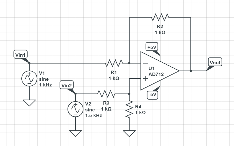
A schematic for simulating the behaviour of a differential op-amp.
This schematic produces the following results:
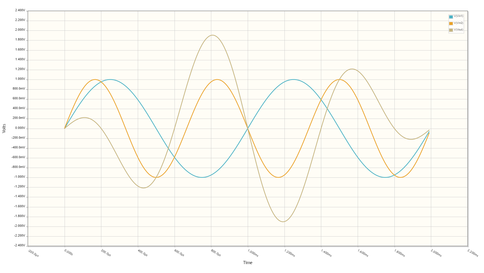
A graph Vout vs. Vin1 and Vin2 for a op-amp configured as a differential amplifier.
Integration Amplifiers
An integration amplifier performs mathematical integration on the input signal – It’s output voltage is proportional to the integral of the input voltage w.r.t. time. The below schematic shows an ideal op-amp based integrator.
An op-amp configured as an ideal integrator.
Eq. \(\ref\) shows the relationship between input and output voltage.
However, this circuit is normally not practical in real world situations. Any errors such as the output offset voltage and input bias current (which all op-amps invariably have), as well as a non-perfect input signal with small amounts of DC bias, will cause the output to drift, until it reaches saturation.
A way to fix this problem is to insert a high-valued feedback resistor, \(R_f\) , to limit the DC gain, as well as a resistor, \(R_\) , on the non-inverting input terminal to compensate for the input bias current.
An op-amp configured as a non-ideal (real world) integrator, with feedback resistor \(R_f\) to slowly remove DC offset and \(R_\) to compensate for input bias current.
\begin v_ &= \frac<1> \int_0^t v_\ dt \\ R_ &= R_i\ ||\ R_f ||\ R_L \\ V_E &= \left(\frac + 1\right) V_ \end
Differentiator Amplifiers
TODO: Add content here.
Transconductance Amplifiers
A transconductance amplifier is an op-amp topology which is used to convert a voltage into a current. Coincidentally, it is also known as a voltage-to-current converter.
A basic transconductance amplifier can be built with an op-amp in a non-inverting configuration.
A transconductance amplifier is useful creating an industry standard 4-20mA (or 0-20mA) current-loop signal. The input voltage can come from something like a potentiometer or microcontroller (coupled with either using a VDAC peripheral or PWM/RC-filter technique to create a variable voltage).
One disadvantage with this design is that the current output is not ground referenced, that is, ground is not used as the return path for the current. This complicates the wiring.
Transimpedance Amplifiers
See the Photodiodes page for information on how to design a transimpedance amplifier to convert a photodiodes output current signal into a voltage.
Current Sources
An op-amp can be easily wired up with a MOSFET and sense resistor to make a voltage controlled current source. See Current Sources And Sinks: Op-amp Current Sink for info on how to make an op-amp current source, including schematics, equations and worked examples.
 for more info.](https://blog.mbedded.ninja/electronics/components/current-sources-and-sinks/current-sink/op-amp-current-sink-schematic.png)
Schematic of an op-amp based current sink. See Current Sources And Sinks: Op-amp Current Sink for more info.
Summing Amplifiers
Op-amps can be used to sum (add) voltages together. There are called summing amplifiers.
Summing amplifiers are used for things such as:
- Mixing audio signals: Audio mixers can be made from summing amplifiers, which combine multiple audio tracks together (e.g. singing with guitar, piano and drums).
- Creating a DAC: Many inputs with resistances following a \(2^n\) pattern are used. These days however you should probably just buy a dedicated DAC IC!
- Level-shifting: For example, shifting a +-5V signal to 0-3.3V for input into a DAC. A two input summing amplifier can do this, with one input being the AC signal you want to level-shift and the other input being a fixed DC offset. Combined with the gain of the op-amp you can both offset and scale the signal.
Inverting Summing Amplifier
The below schematic shows a inverting summing amplifier with three inputs.
A summing amplifier with three inputs.
How Does The Inverting Summing Amplifier Work?
The current \(i_f\) going through the resistor \(R_f\) is just the sum of the currents going through resistors \(R_i\) .
\begin i_f &= — (i_1 + i_2 + i_3) \\ \end
The inverting input of the amplifier is at “virtual ground”.
Again, because the inverting input is at \(0V\) , the voltage \(v_\) is just:
Substitute Eq. \(\ref\) into Eq. \(\ref\) , and then simplify a little:
And there we have it! Eq. \(\ref\) shows you [^summing-amplifier-inverting] works as an inverting summing amplifier for three input voltages \(v_1\) , \(v_2\) , and \(v_3\) . Note that aside from summing, the inverting summing amplifier also applies the negative gain \(- \frac\) , just like a standard [^_inverting_amplifiers, inverting amplifier]. You can make \(R_f\) equal to \(R_i\) if you don’t want any gain, but you can’t avoid the inverting part. If you don’t want it to invert (perhaps your using a single-sided supply?), then take a look at the [^_non_inverting_summing_amplifier, non-inverting summing amplifier].
Whilst common, the resistors \(R_i\) do not need to be equal. If they are not equal, the circuit in [^summing-amplifier-inverting] is called a scaling summing amplifier. Each input voltage is scaled by a value determined by it’s input resistance before being summed together.
Non-inverting Summing Amplifier
The non-inverting summing amplifier is similar to the inverting summing amplifier except that it does not invert the input voltages. The advantages and dis-advantages of the non-inverting vs the inverting summing amplifier are highlighted below:
Advantages
- Does not invert the input signals (this might actually be a dis-advantage, depending on the application!)
- May only need a single-ended voltage supply (depending on the voltage ranges of the inputs).
- Higher input impedance
Disadvantages
- More complicated gain equation/resistor values (because there is no virtual ground at the inputs).
- Unused inputs cannot be left floating, they must be grounded (more on this below).
The below schematic shows a non-inverting summing amplifier with three inputs.
A non-inverting summing amplifier with three inputs.
If all the input resistors are equal ( \(R_1 = R_2 = R_3 = R\) ), the gain equation is:
How Does The Non-Inverting Summing Amplifier Work?
Because we have no nice virtual ground at the non-inverting input, we have to analyze the non-inverting summing amplifier a little differently to the inverting version. First, use Kirchhoff’s current law:
\begin i_1 + i_2 + i_3 = 0 \\ \end
Let’s call the voltage at the non-inverting pin \(v_+\) . We can then write replace the currents above with the voltage difference divided by the resistance:
Let’s assume the input resistors are equal ( \(R_1 = R_2 = R_3 = R\) ), then simplify and solve for \(v_+\) :
\begin \frac<1> ( v_1 — v_+ + v_2 — v_+ + v_3 — v_+ ) &= 0 \nonumber \\ v_1 + v_2 + v_3 — 3v_+ &= 0 \nonumber \\ v_+ = \frac <3>\\ \end
So now we have an equation for \(v_+\) in terms on the input voltages. As described in the [^_non_inverting_amplifiers], the equation for a non-inverting amplifier is:
Substituting in \(v_+\) we get the final equation for a 3-input non-inverting summing amplifier:
Notice the \(3\) . This scaling factor is equal to the number of inputs the non-inverting summing amplifier has, so remember that the scaling factor changes if you add/remove inputs!
WARNING: Unused inputs into a inverting summing amplifier can be left floating. Unused inputs into a non-inverting amplifier CANNOT be left floating, they need to be tied to ground (0V).
Level Shifters
Op-amps can be used to perform level-shifting. The concept of level-shifting is very similar to what is achieved by [^_summing_amplifiers, summing amplifiers].
Simulation example for an op-amp based level shifter.
The below schematic shows a op-amp based level shifter which converts a \(\pm 5.0V\) signal into a \(0-3.3V\) signal, suitable for passing into a microcontrollers DAC for digital conversion and processing (microcontrollers often run of \(+3.3V\) , hence that is also a common choice for the reference voltage of the DAC). If you used rail-to-rail op-amps, you might be able to get away with lowering the voltage rails for the op-amp to \(\pm 5.0V\) .

Schematic of a level-shifting circuit that converts a \(\pm 5.0V\) signal into a \(0-3.3V\) signal.
![Simulation results of the level-shifting circuit shown in [^level-shifter-sim-schematic]. You can clearly see that the `\(\pm 5.0V\)` signal has been level-shifted to the range `\(0-3.3V\)`. Because the input is connected to the non-inverting input of the op-amp, the output is in phase with the input signal (i.e. not inverted).](https://blog.mbedded.ninja/electronics/components/op-amps/level-shifter-sim/out.png)
Simulation results of the level-shifting circuit shown in [^level-shifter-sim-schematic]. You can clearly see that the \(\pm 5.0V\) signal has been level-shifted to the range \(0-3.3V\) . Because the input is connected to the non-inverting input of the op-amp, the output is in phase with the input signal (i.e. not inverted).
Ideal Diodes/Rectifiers
Basic Ideal Diode/Rectifier
An op-amp can be combined with a regular diode to make an “ideal diode” (also called a superdiode 2 , precision rectifier, or half/full-wave rectifier), one that rectifies and has no voltage drop. Ideal diode circuits are useful when:
- You have to rectify a signal with precision (the forward voltage drop across the diode is unacceptable).
- You have to rectify a small signal, whose amplitude is less than a forward diode drop.
The below schematic shows the most basic form of an ideal diode (a.k.a. a half-wave rectifier). Because feedback to the inverting pin is taken from the load ( \(v_\) ), the op-amp will drive it’s output to whatever is needed to make the output voltage the same as the input voltage (when \(v_\) is positive), thereby compensating for the forward voltage drop of the diode. When \(v_\) is negative, the op-amp will try as hard as it can to lower the output voltage, but this will be blocked from the output by the diode, providing the rectifying action.
A basic “ideal diode” with no forward voltage drop, made from an op-amp and a standard diode. Also called a half-wave rectifier.
The below graph shows the response of the basic ideal diode circuit.
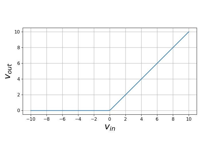
The response of the basic “ideal diode”/half-wave rectifier circuit shown in [^ideal-diode-basic].
The ideal diode is only ideal up to a point. It is not limited by the bandwidth and max. slew rates of the op-amp, which is typically much less than of a basic diode! There is also an issue with slew rates with the above circuit. As soon as \(v_\) goes negative, the op-amp will “saturate” and swing it’s output to the maximum negative voltage. This will cause some delay on the output (limited by the slew rate) when the input once again goes positive.
TIP: The standard diode in the ideal diode circuit can be replaced by a Schottky diode for a quick-and-easy speed improvement (Schottky diodes have faster switching speeds).
Improved Half-wave Rectifier
The below schematic shows an improved half-wave rectifier with additional circuitry to prevent the op-amp from saturating when in the blocked part of the cycle 3 . Note that this also is an inverting half-wave rectifier – it rectifies the negative half of the input and outputs it as a positive wave on the output.
An improved ideal diode/half-wave rectifier.
The gain of the half-wave rectifier above is:
Basic op-amp based sample-and-hold circuit.
Important Variables
Sorted by function.
Common-Mode Input Voltage Range
The common-mode input voltage range is the range of voltages that can appear at the input to the op-amp and it still work correctly. For standard single-supply op-amps, the typical range is approximately \(0V\) to \(V_+ — 1.5V\) . Note how it includes the most negative rail \(V_-\) (which is 0V for a single-supply op-amp) but only gets within 1.5V of the most positive rail, \(V_+\)
Input Offset Voltage (Vos/Vio)
The input offset voltage \(V_\) (or sometimes called \(V_\) ) is the voltage difference required between the two input pins to force the output to 0. It is a DC measurement parameter. In an ideal op-amp, the op-amp only amplifies a difference between the inputs, and so the output is 0V when the difference is 0V, hence the input offset voltage is 0V. However, real-world op-amps always have some unavoidable differences in the internal components that make up the op-amps (specifically, in the input differential stage of the internal circuitry), and thus the inputs are not perfectly identical. The below circuit shows how the input offset voltage is modelled as a voltage source in series with one of the inputs of an ideal op-amp.
The input offset voltage is modelled as a voltage source in series with one of the inputs of an ideal op-amp (it doesn’t matter which input, as the input offset voltage can be positive or negative).
A non-zero input offset voltage results in gain errors between the input and output of a op-amp. The input offset voltage is typically in the following ranges:
- 1-5mV for good general purpose op-amps, 5-15mV for really bad ones.
- 200uV-1mV for specialized low input offset voltage op-amps
- 10uV-200uV for the best “ultra” low input offset voltage op-amps.
- < 1uV for chopper-stabilized (auto-zero) op-amps.
For example, the general purpose LM324 has a typical input offset voltage of 2mV and a maximum of 3mV, at \(T_A = 25°C\) 4 . “Low” input offset voltage op-amps will have a \(V_\) in the range of 50-200uV. For example, the OPAx196 family of op-amps has a max. \(V_: 100uV\) 5 .
Input offset voltages vary by op-amp transistor technology. Bipolar op-amps typically have the lowest input offset voltage, followed by CMOS and the BiFET op-amps 6 .
Input Offset Voltage Drift
The input offset voltage varies with both temperature and time (drift). The variation with temperature is usually represented by \(T_C V_\) (I’ve also seen \(\Delta V_/\Delta T\) used 7 ). Typical temperature drift for precision op-amps is in the range of \(1-10uV^<\circ>C\) 8 . The venerable LM324 has a \(T_C V_ = 7uV^<\circ>C\) (max) 7 .
The change of input offset voltage with time is called aging. Aging is normally specified in \(uV/1000hours\) . But since aging is a physical process that follows the “random walk pattern” (Brownian motion), it is more accurate to describe it proportional to the square root of elapsed time.
Some op-amps are trimmed by the manufacturer after the op-amp is packaged. Performing trimming after packaging prevents any production-line effects from effecting the input offset voltage. One such example is the family of AD8601, AD8602 and AD8604 op-amps from Analog Devices (they call it DigiTrim). The offset is trimmed with a special digital code using no extra pins (i.e. reuses existing op-amp pins). Once programmed, poly-silicon fuses are blown to permanently set the trim values 8 .
Trimming Input Offset Voltage
If your op-amp lacks a dedicated trim pin, you can make your own trimming circuit as shown below. This is for an op-amp in the inverting configuration. \(VR1\) is a potentiometer, manually adjusted until it cancels out the op-amps input offset voltage.
A popular way of performing external input offset voltage trimming with a inverting op-amp.
The maximum input offset voltage you can compensate for with this circuit is given by Eq \(\ref\) 8 .
Input Bias Current (Ib+ and Ib-)
The input bias current \(I_\) and \(I_\) describe the currents that flow in and out of the op-amps input pins. In an ideal op-amp, no current flows into/out of the input pins (the op-amp has infinite input impedance). In reality, always some small amount of current will flow. Typical input bias currents range from 1-10nA. Special “low input bias current” op-amps can have much lower values. For example, the Texas Instruments OPA396 has a typ. \(I_B = \pm 10fA\) at \(25^<\circ>C\) ! This increases to approx. \(\pm 4pF\) across it’s entire temperature range (typical) 9 .
The amount and behaviour of input bias current depends on the op-amp transistor technology. A FET-based op-amp’s input bias current will approximately double with every 10°C rise in temperature 10 11 .
Input bias currents are a problem because these currents will flow through external circuitry connected to the op-amps inputs. This current when flowing through resistors and other impedances will create unwanted voltages which will increase the systematic errors. Finding an op-amp with a low input bias current can be important for a high sensitivity transimpedance amplifier, such as one connected to a photodiode.
Input Impedance
The input impedance is the internal resistance to ground from the two input pins. In an ideal op-amp, this value is infinite. For most op-amps, this value is somewhere between 1-10MΩ.
Gain-Bandwidth (GBW) Product
The gain-bandwidth product (initialised as GBWP, GBW, GBP or GB) is an important parameter which puts a limit on the maximum gain and frequency an op-amp can operate at. An op-amp’s maximum possible gain reduces as the frequency of the signal increases. The multiplication of the gain with the frequency gives the gain-bandwidth product, which is relatively constant for a particular op-amp.
Hence if the gain bandwidth of a particular op-amp is 1Mhz, and the gain is 10, the maximum frequency that the op-amp can operate linearly at (still provide a gain of 10) is at 100kHz. Or if the gain was set to 100, then the maximum frequency is 10kHz. This also means that an op-amp acts as a low-pass filter, as the gain drops for very high frequencies. Like wise for a GBW of 1MHz, is the gain was just 1 (i.e. acting as a buffer/follower), then it should be able to operate up to frequencies of 1MHz.
An example of an ultra-high gain bandwidth is 1700MHz, which are present in ‘Wideband CFB» op-amps, designed for applications such as RGB line drivers (such as the OPA695). A ’normal’ GBW can be anywhere between 100kHz and 10MHz. A low gain-bandwidth is around 1kHz (reminiscent of less advanced, older op-amps). Remember gain is unit-less (V/V), so gain bandwidth is expressed as a frequency only. Not realising this can be confusing! The GBW product is closely related to the [^_slew_rate, slew rate].
High Level Output Voltage
The high level output voltage ( \(V_\) ) defines the highest voltage which the op-amp can drive the output to (with respect to the power supply \(V_+\) ).
Low Level Output Voltage
\) ) defines the lowest voltage which the op-amp can drive the output to. The LM324 is rumoured to only be able to drive the output near ground if it is sourcing current, but only to 0.5V minimum if sinking (see this EDA Forum post, LM324 Opamp Gain Instability).
Slew Rate
The slew rate of an op-amp defines the maximum rate the output voltage can change with respect to time. In an ideal op-amp, this would be infinite. It has the SI units \(V/s\) , and is commonly expressed in \(uV/s\) . It can be thought of as the slope of the output waveform if one of the inputs of the input was subjected to a step voltage change.
Op-amps have a limited output slew rate due to internal compensation capacitor combined with a finite output drive current. Charing a capacitive output with a constant current (a good approximation) gives a linear increase in voltage (recall that the equation relating voltage to current for a capacitor is \(i = C \frac
\) ).
The plot below shows how the non-infinite slew rate of an op-amp distorts the shape of an input square-wave “pulse”. The slew rate of \(0.4V/us\) (which is not particularly good by any standard) of the “jellybean” LM324 op-amp was used in this plot 12 .
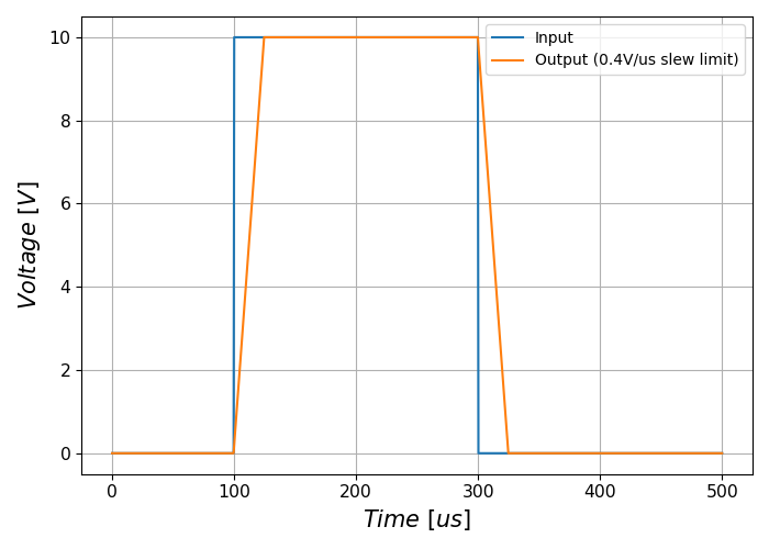
Plot showing the effect an op-amps slew rate on a input square wave. Slew rate was chosen to be equal to the LM324’s of 0.4V/us 12 .
The max. slew rate of an op-amp limits the amplitude of output waveforms it can produce at high frequencies without distortion. This parameter usually increases as the GBW of the op-amp increases. Higher slew rate op-amps also tend to have higher quiescent currents.
Slew Rate Equation
The maximum frequency of a signal that an op-amp can output before it gets distorted because of it’s maximum slew rate limit is given by the following equation:
\begin SR = 2\pi f_ V_P \end
where:
\(SR\) is the slew rate, in \(Vs^<-1>\)
\(f_\) is the maximum frequency (of a sine wave) that is allowed before distortion, in \(Hz\)
\(V_P\) is the peak voltage of the sine wave (i.e. amplitude, or half the peak-to-peak voltage), in \(V\)
Proof
A sine wave at frequency \(f\) and has peak voltage \(V_P\) is described with the equation:
\begin f(t) = V_P \sin (2\pi f t) \end
The slope at any point in time \(t\) is found by taking the derivative. As per standard derivative rules, the derivative of \(\sin\) is \(\cos\) and you multiply the function by what is inside the \(\sin\) :
\begin \frac
= 2\pi f V_P \cos (2\pi f t) \end
We want to find the maximum slope, \(max\left(\frac
\right)\) . We know that the maximum value of any \(\cos\) function is \(1\) , so we can simplify to:
\begin max\left(\frac
\right) = 2\pi f V_P \end
This maximum slope \(max\left(\frac
\right)\) is the maximum slew rate of the op-amp \(SR\) . Hence:
\begin SR = 2\pi f_ V_P \end
Finding the max. frequency of the LM324 due to slew rate limitations.
So just as an example, the jellybean LM324 with a slew rate of \(0.4V/us\) can generate a \(10V\) peak ( \(20V\) peak-to-peak) waveform of the following frequency before distortion:
Slew Rate Effects On Sine Waves
The below plot shows different levels of distortion for a 10V (peak) 20kHz sine wave when it is generated by an op-amps with different slew rates. The jellybean LM324 slew rate of \(0.4V/us\) is shown (which outputs a triangle wave!) along with a slightly better \(1.0V/us\) (which just clips the sine wave). The minimum slew rate required to prevent any distortion of the sine wave is \(1.26V/us\) .
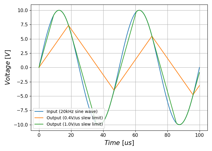
Plots showing the distortion of a 10V (peak) 20kHz sine wave when subjected to different op-amp slew rates.
Quiescent Current
The quiescent current (current with no load, device in steady-state) is generally constant over the total rated supply voltage range. Obviously, if there is a load on the op-amp, the current drawn through the power pins (the supply current) will be the sum of the quiescent current and the current going through the load.
Quiescent currents for standard op-amps are typically between 1.5-4mA. A ’low-power’ op-amp has a typical quiescent current between 0.5-1.5mA (such as the LM258N ). Then there are ultra-low power op-amps that only draw 5-20pA (such as the LMC6464 ). You normally sacrifice slew-rate and gain-bandwidth for ultra-low power. Likewise, higher gain-bandwidth and higher slew rate op-amps typically have larger quiescent currents.
Cascading Op-Amps
Cascading op-amps is concept when the output of one op-amp is connected to the input of another. There can be an arbitrary number of op-amps in the cascade, but usual limits are 3-4.
For a fixed-gain, cascading op-amps can also be used to increase the bandwidth, as each individual op-amp now can operate at a lower gain and therefore has a larger bandwidth as defined by the gain-bandwidth product. Note though that each additional op-amp added to increase the bandwidth gives diminishing returns. Also important to note that op-amp bandwidth is defined as the -3dB gain points. Hence the bandwidth does not stay the same (total bandwidth gets smaller) when two identical op-amps are cascaded, as these will now the -6dB points. A practical limit for fixed-total-gain increased-bandwidth cascading is about 3-4 op-amps.
The Gain
When cascading op-amps, the total gain is the product of all of the individual op-amps gains, i.e.:
\begin A_ = A_0 A_1 A_2 . A_n \end
The Bandwidth
The bandwidth of cascaded op-amps is not as simple to calculate as the gain.
If all of the op-amps are identical, then the following equation can be used:
where: \( BW_ \) = the total bandwidth of the cascaded op-amp system
\( BW \) = the bandwidth of the individual op-amps (remember, they have to be identical)
\( N \) = the number of op-amps in the cascaded system
The above equation gives diminishing returns with every additional op-amp added.
Feedback Resistor Values
As a rule-of-thumb, you should use the lowest acceptable resistances in op-amp feedback paths to reduce instabilities.
Types Of Op-Amps
General Purpose
General purpose op-amps typically have parameters in the following ranges:
- Gain Bandwidth Product: 1MHz
- Input Bias Current: 15pA
- Input Voltage Offset: 1mV
- Output Current: 20-50mA
- Icc: 1mA
Rail-to-Rail Op-Amps
\) ) parameter in the op-amp’s datasheet. For “rail-to-rail” op-amps, this will usually be about 100-200mV about ground at normal load currents.
This also means that a rail-to-ral single-supply op-amp cannot output 0V. To achieve a true ground output, you need a negative voltage supply. There are dedicated ICs designed to provide a small negative power supply to op-amps so that they can output true ground. One such example is the Texas Instruments LM7705, a “Low Noise Negative Bias Generator”. This IC only generates -230mV, which allows the designer to use CMOS-based op-amps which usually have a maximum supply voltage of 5.5V.
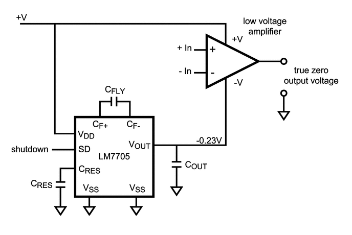
The typical application schematic for the Texas Instruments LM7705, a ‘Low-Noise Negative Bias Generator’ for the negative supply of an op-amp. This allows the op-amp to output true 0V. Image from http://www.ti.com/.
Micropower Op-Amps
Micropower is a termed used for extremely low quiescent current op-amps that are designed for battery or energy recovery-based power supplies. The supply current of micropower op-amps is typically within the range of 50-100uA at a supply voltage of 2-10V. Because they are designed for battery-based systems, they are also commonly single-supply op-amps.
Instrumentation Amplifiers
Instrumentation amplifiers are analog voltage amplifier circuits that, although are drawn the the same symbol as an op-amp, are typically made up internally from three op-amps (and passives). You can either make an instrumentation amplifier out of discrete op-amps or purchase a instrumentation amplifier IC which contains all the op-amps within the same chip.
Manufacturer Part Number Families
INA ** INAx126: Precision instrumentation amplifiers by Texas Instruments. The INA126 has one amplifier per package, the INA2126 has two. ** INA290: Precision current-sense amplifier.
LM741: Very popular and old “741” style op-amp produced by Texas Instruments, ON Semiconductor and Rochester Electronics.
LT: The prefix Linear Technology (now Analog Devices) uses for their range of op-amps. ** LT1006: Precision, single-supply op-amp. ** LT1077: Micropower, single-supply op-amp. ** LT1167: Instrumentation amplifier.
MAX: Op-amps by Maxim. ** MAX4194: Instrumentation amplifier.
OP07: Analog Devices/Texas Instruments ranges of low input offset voltage op-amps. ** OP07C: ±3-18V VCC, -40 to +85°C industrial temp. range *** OP07CP: DIP-8 package *** OP07CS: SOIC-8 package ** OP07D: ±4-18V VCC ** OP07E: 0 to 70°C commercial temp. range
OPA: Texas Instruments (previously Burr-Brown) family of op-amps. ** OPAx187: Zero-drift 36V rail-to-rail op-amps. Includes the OPA187 (1 op-amp), OPA2187 (2 op-amps) and OPA4187 (4 op-amps). ** OPA241: Single-supply ** OPA251: Dual-supply ** OPA27: Texas Instruments (previously Burr-Brown) family of ultra-low noise, precision op-amps. Internally compensated for unity-gain stability. ** OPA37: Uncompensated version of the OPA27.
TLE202: Texas Instruments family of “high-speed low-power” precision operational amplifiers. Belong to the Excalibur family of TI op-amps which uses “isolated vertical PNP transistors” to give unity-gain bandwidth and slew rate improvements.
TLV: Texas Instruments family of op-amps.
Vsupply is voltage from Vdd/Vcc to Vss/Vee.
The Different Types Of Gain, Explained
\) ) is the gain of the op-amp without any feedback.
Closed loop gain \(G_V\) is the over-all gain of the op-amp with feedback.
How the open-loop and closed-loop gain of an op-amp changes with increasing frequency.
We can generalize the circuit of an op-amp with negative feedback to the block diagram shown below.
A block diagram showing a generalized op-amp configuration with negative feedback.
From the above block diagram we can write an equation for \(v_\) :
What we are really interested is an equation for the closed-loop gain \(G_V\) which is equal to \(\frac>>\) …all we need to do is to re-arrange the equation as shown below:
And so we come to an equation for the closed loop gain \(G_V\) as:
We can take this one step further, since normally the open-loop gain \(A\) for an op-amp is very large, in the range of \(100,000\) to \(1,000,000\) . With that, we can simply the closed loop gain to be:
\begin G_V &\approx \frac<1> \end
- Open-loop gain: \(A\)
- Loop gain: \(-AB\)
- Closed-loop gain: \(\approx \frac<1>\)
Examples
Below are some examples of op-amps that stand out from the crowd for some reason, be it popularity, years in service, or functionality wise.
AD860x
LM32x
A common family of op-amps that has been around for along time, they can operate of a single supply and can swing right to ground, but cannot swing to the rail voltage. The LM321 has one op-amp, the LM328 has two (dual), and the LM324 has 4 (quad).
LM833
One of the cheapest ‘audio’ op-amps available (about US$0.20 as of 2011). Features a high GBW for it’s price.
OPA695
US$3.50 (1) This is a ultra-wideband, current-feedback op-amp. If you need an op-amp with a ridiculously high gain-bandwidth product, this is along the lines of what you want to use. It has a GBW of 1700Mhz and a maximum slew-rate of 4300V/us.
A op-amp with a “ultra” low input offset voltage (resistors are trimmed at production time to achieve this), guaranteed to be no more than 75uV. This op-amp also features offset nulling pins to further reduce the input offset voltage by performing trimming once the op-amp is installed in a circuit.
Negative Voltage Rails
Dedicated charge-pump topology power supply ICs are available that supply a small negative voltage to the op-amps V- pin.
Isolation Amplifiers
Isolation amplifiers provide galvanic isolation between the input (sensor) and output (measurement circuitry). They are used to protect the sensor measurement and recording circuitry (e.g. a microcontroller with on-board ADC) from dangerously high voltages at the sensor, and also the opposite, to protect the sensor environment from potentially dangerous voltages on the rest of the system.
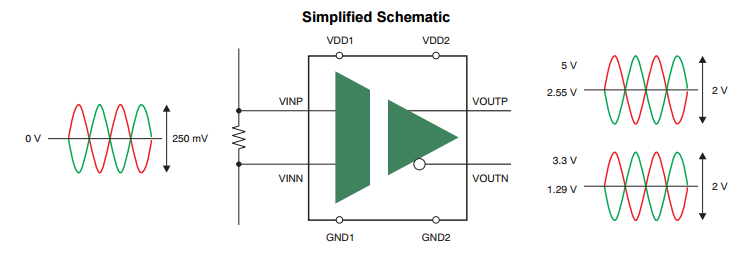
A simplified schematic of the Texas Instruments AMC1200, a fully-differential isolated amplifier. Image from http://www.ti.com/.
A common application would be to isolate and amplify the voltage across a current-sense resistor on a high-power motor, or to protect humans with medical sensors connected to them from the measurement system.
Basic isolation amplifiers require two power supplies (one for each side of isolation), while others incorporate built-in transformers so that you only have to provide one power source.
Input Resistors
One of the first things you learn about an op-amp is that the input impedance on the input pins are very large (ideally infinite). So naturally you would start to question why resistors would be connected to the input pins of an op-amp like shown below.
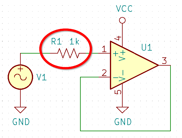
Schematic showing a resistor on the positive input to a op-amp.
These input resistors serve to limit the input current if the voltage on the input pin goes above \(V_\) . Most op-amps have protection/clamping diodes from the input pins to \(V_\) (typically you can determines this if in the datasheet the input pins max voltage is rated to \(V_ + 0.3V\) , which is one diode voltage drop). If there was no resistor there, the built-in diode would conduct and sink a large current from the input pin to \(V_\) , possibly damaging the op-amp. The resistor limits this current to a safe value.
Offset Nulling Circuits
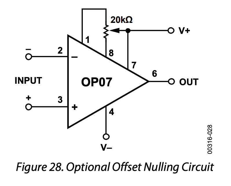
Some op-amps which are designed to have very low input offset voltages also come with offset nulling pins to further trim the input offset voltage once the op-amp is installed in circuit. The OP07 is one op-amp which has these pins. Typically, a \(10-50k\Omega\) potentiometer is connected across these pins with the wiper going to \(V_\) , as shown below.
Negative Impedance Converters (NICs)
What Is A NIC?
A negative impedance converter (NIC) is a clever op-amp circuit which creates negative impedance (you might be wondering what negative impedance actually is, more on this later). A NIC can be constructed from an op-amp and a few passive components as shown in the following schematic:
Schematic of a negative impedance converter (NIC) created from an op-amp and a few passive components.
Typically the two resistances are the same ( \(R1 = R2\) ), and then the input impedance \(Z_\) is:
where:
\(Z_\) is the input impedance, in Ohms (\(\Omega\))
\(-Z\) is the impedance of the component connected between the inverting terminal and ground, as shown on the diagram, in Ohms (\(\Omega\))
What Does Negative Impedance Actually Mean?
What does negative impedance actually mean? If \(Z\) is just a simple resistor with resistance \(R\) (the most basic kind of NIC), then the impedance is \(Z_ = -R\) . This means the circuit behaves just like a simple resistor connected to ground, except that the current comes out of the resistor, not into it.
Things get more interesting when you replace this resistor with a capacitor.
TODO: Add explanation of what happens when capacitor is added.
NIC Input Impedance Proof
To prove \(Z_ = -Z\) , we need to find the input current at inverting terminal, and then use \(Z_ = \frac>\) . The input current can be found by application of Ohm’s law and the golden rules of op-amps. Using the rule that the voltage at the two input terminals will be the same, we know the voltage across the impedance \(Z\) is going to be:
Using Ohm’s law, the current through the impedance \(Z\) is therefore:
Because there is no current going into the inverting terminal of the op-amp, this current \(I_Z\) must also be flowing through \(R2\) :
Now knowing the voltage at the inverting terminal and the current through \(R2\) we can write an equation for the voltage at the output of the op-amp:
Now that we know the voltage on both sides of \(R1\) we can find the voltage across it:
Now we know the voltage across \(R1\) we can find the current going through it using Ohm’s law:
» Because the voltage on the right-hand side of `\(R1\)` is higher, this current is flowing right-to-left. Since no current flows into the inverting terminal of the op-amp, this also must be current flowing «out» of the input terminal. Thus:
Knowing the input current and voltage, we can finally write an equation for \(Z_\) :
Chopper-Stabilised Op-Amps
Capacitive Loading
Industry Standard Package Pinouts For Op-Amps
Op-amps are usually packaged in industry standard through-hole and surface mount packages. For many of these packages, there are industry standard pinouts which means you can easily find pin-compatible alternatives for any given op-amp. This section aims to illustrate some of these industry standard pinouts.
For 8-pin packages:
The standard pinout for two op-amps in an 8-pin package. This includes the DIP-8, TSSOP-8, SOIC-8 and MSOP-8 component packages.